Timer/counter1, Atmega161(l) – Rainbow Electronics ATmega161L User Manual
Page 49
49
ATmega161(L)
1228C–AVR–08/02
•
Description of wake-up from Power-save mode when the timer is clocked
asynchronously: When the interrupt condition is met, the wake-up process is started
on the following cycle of the timer clock, that is, the timer is always advanced by at
least 1 before the processor can read the counter value. The Interrupt Flags are
updated three processor cycles after the processor clock has started. During these
cycles, the processor executes instructions, but the interrupt condition is not
readable and the interrupt routine has not started yet.
•
During asynchronous operation, the synchronization of the Interrupt Flags for the
asynchronous timer takes three processor cycles plus one timer cycle. The timer is
therefore advanced by at least 1 before the processor can read the timer value,
causing the setting of the Interrupt Flag. The output compare pin is changed on the
timer clock and is not synchronized to the processor clock.
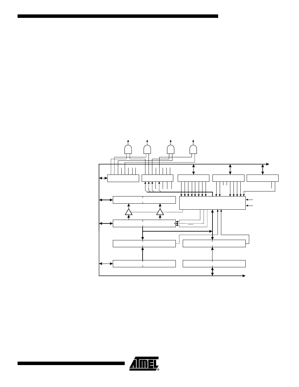
Timer/Counter1
Figure 35 shows the block diagram for Timer/Counter1.
Figure 35. Timer/Counter1 Block Diagram
The 16-bit Timer/Counter1 can select clock source from CK, prescaled CK or an exter-
nal pin. In addition, it can be stopped as described in “Timer/Counter1 Control Register
B
–
TCCR1B”. The different Status Flags (Overflow, Compare Match, and Capture
Event) are found in the Timer/Counter Interrupt Flag Register (TIFR). Control signals
are found in the Timer/Counter1 Control Registers (TCCR1A and TCCR1B). The inter-
rupt enable/disable settings for Timer/Counter1 are found in the Timer/Counter Interrupt
Mask Register (TIMSK).
When Timer/Counter1 is externally clocked, the external signal is synchronized with the
Oscillator frequency of the CPU. To assure proper sampling of the external clock, the
minimum time between two external clock transitions must be at least one internal CPU
TOIE0
TOIE1
OCIE1A
OCIE1B
TICIE1
TOIE2
OCIE2
OCIE0
TOV0
TOV1
OCF1A
OCF1B
ICF1
TOV2
OCF2
OCF0
TIMER INT. FLAG
REGISTER (TIFR)
CONTROL
LOGIC
TIMER/COUNTER1 (TCNT1)
TIMER INT. MASK
REGISTER (TIMSK)
T/C1 INPUT CAPTURE REGISTER (ICR1)
T/C1 OVER-
FLOW IRQ
T/C1 COMPARE
MATCHA IRQ
T/C1 COMPARE
MATCHB IRQ
T/C1 INPUT
CAPTURE IRQ
8-BIT DATA BUS
16 BIT COMPARATOR
TIMER/COUNTER1 OUTPUT COMPARE REGISTER A
16 BIT COMPARATOR
TIMER/COUNTER1 OUTPUT COMPARE REGISTER B
CAPTURE
TRIGGER
CK
0
7
8
15
0
7
8
15
0
7
8
15
0
7
8
15
0
7
8
15
0
7
8
15
T/C CLEAR
T/C CLOCK SOURCE
UP/DOWN
T/C1 CONTROL
REGISTER A (TCCR1A)
T/C1 CONTROL
REGISTER B (TCCR1B)
FOC1A
FOC1B
COM1A1
COM1A0
COM1B1
COM1B0
PWM11
PWM10
ICNC1
ICES1
CTC1
CS12
CS11
CS10
PSR2
PSR10
SPECIAL FUNCTIONS
IO REGISTER (SFIOR)
TOV1
OCF1B
OCF1A
ICF1
TOV2
OCF2
OCF0
TOV0
T1