Enter programming mode, Chip erase, Atmega161(l) – Rainbow Electronics ATmega161L User Manual
Page 119
119
ATmega161(L)
1228C–AVR–08/02
Enter Programming Mode
The following algorithm puts the device in Parallel Programming mode:
1.
Apply 4.5 - 5.5V between V
CC
and GND.
2.
Set RESET and BS pins to “0” and wait at least 500 ns.
3.
Apply 11.5 - 12.5V to RESET, and wait for at least 500 ns.
Chip Erase
The Chip Erase will erase the Flash and EEPROM memories plus Lock bits. The Lock
bits are not reset until the Program memory has been completely erased. The Fuse bits
are not changed. A Chip Erase must be performed before the Flash is reprogrammed.
Load Command “Chip Erase”
1.
Set XA1, XA0 to “10”. This enables command loading.
2.
Set BS1 to “0”.
3.
Set DATA to “1000 0000”. This is the command for Chip Erase.
4.
Give WR a negative pulse. This starts the Chip Erase. RDY/BSY goes low.
5.
Wait until RDY/BSY goes high before loading a new command.
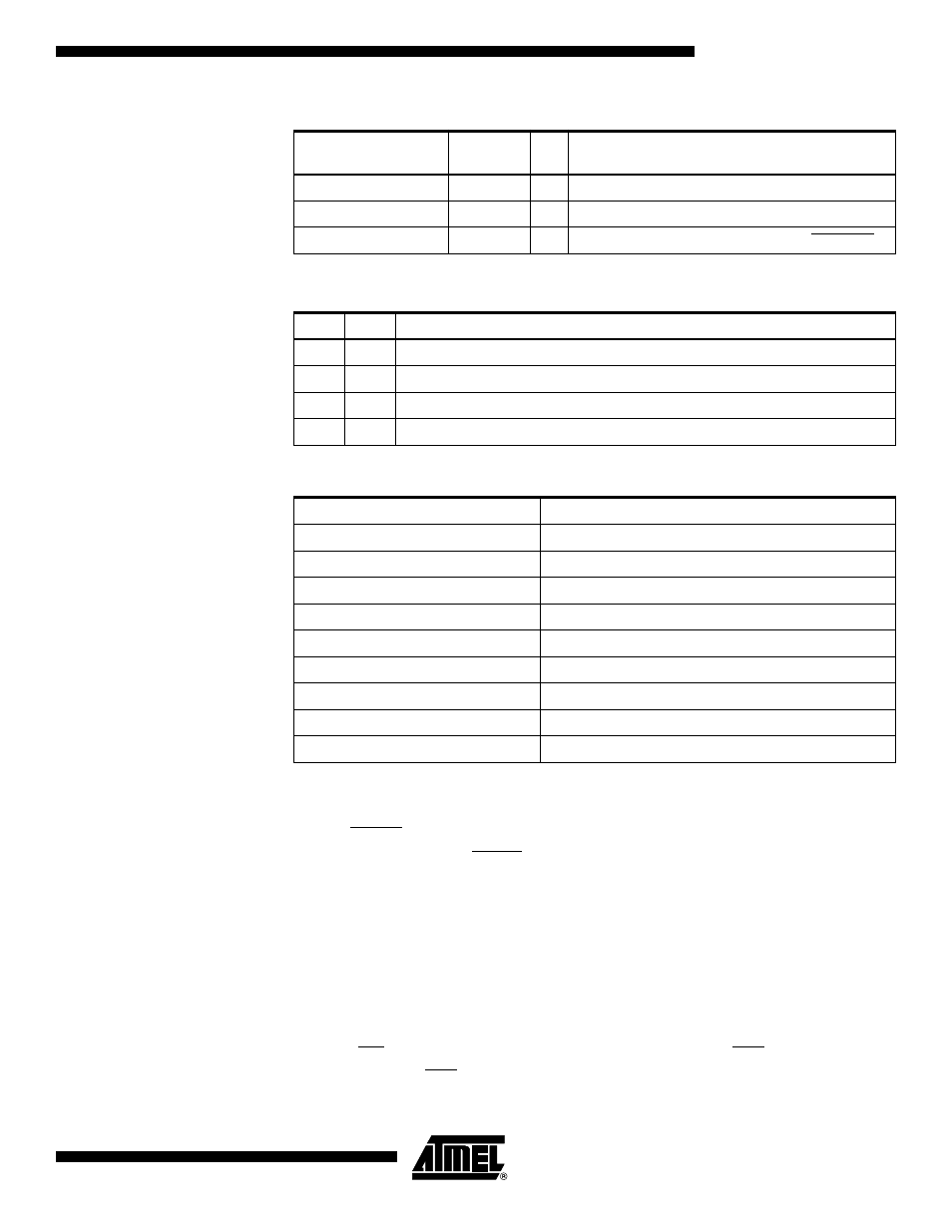
PAGEL
PD7
I
Program Memory Page Load
BS2
PA0
I
Byte Select 2 (Always low)
DATA
PB7 - 0
I/O
Bi-directional Data Bus (Output when OE is low)
Table 43. XA1 and XA0 Coding
XA1
XA0
Action when XTAL1 is Pulsed
0
0
Load Flash or EEPROM Address (High or low address byte determined by BS1)
0
1
Load Data (High or low data byte for Flash determined by BS1)
1
0
Load Command
1
1
No Action, Idle
Table 44. Command Byte Bit Coding
Command Byte
Command Executed
1000 0000
Chip Erase
0100 0000
Write Fuse bits
0010 0000
Write Lock bits
0001 0000
Write Flash
0001 0001
Write EEPROM
0000 1000
Read Signature Bytes
0000 0100
Read Fuse and Lock bits
0000 0010
Read Flash
0000 0011
Read EEPROM
Table 42. Pin Name Mapping
Signal Name in
Programming Mode
Pin Name
I/O
Function