Interface to external memory, Mcu control register – mcucr, Extended mcu control register – emcucr – Rainbow Electronics ATmega161L User Manual
Page 84: Atmega161(l)
84
ATmega161(L)
1228C–AVR–08/02
Interface to External
Memory
With all the features the external memory interface provides, it is well suited to operate
as an interface to memory devices such as external SRAM and Flash, and peripherals
such as LCD display, A/D, D/A, etc. The control bits for the external memory interface
are located in two registers, the MCU Control Register (MCUCR) and the Extended
MCU Control Register (EMCUCR).
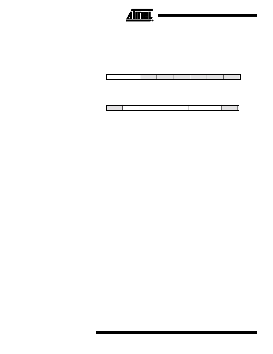
MCU Control Register –
MCUCR
Extended MCU Control
Register – EMCUCR
• Bit 7 MCUCR – SRE: External SRAM Enable
When the SRE bit is set (one), the external memory interface is enabled and the pin
functions AD0 - 7 (Port A), A8 - 15 (Port C), ALE (Port E), WR and RD (Port D) are acti-
vated as the alternate pin functions. The SRE bit overrides any pin direction settings in
the respective Data Direction Registers. See Figure 50 through Figure 53 for a descrip-
tion of the external memory pin functions. When the SRE bit is cleared (zero), the
external Data memory interface is disabled and the normal pin and data direction set-
tings are used
• Bits 6..4 EMCUCR – SRL2, SRL1, SRL0: Wait State Page Limit
It is possible to configure different wait states for different external memory addresses.
The external memory address space can be divided into two pages with different wait
state bits. The SRL2, SRL1 and SRL0 bits select the split of the pages (see Table 28
and Figure 49). As defaults, the SRL2, SRL1 and SRL0 bits are set to zero and the
entire external memory address space is treated as one page. When the entire SRAM
address space is configured as one page, the wait states are configured by the SRW11
and SRW10 bits.
• Bit 1 EMCUCR and Bit 6 MCUCR – SRW11, SRW10: Wait State Select Bits for
Upper Page
The SRW11 and SRW10 bits control the number of wait states for the upper page of the
external memory address space (see Table 27). Note that if the SRL2, SRL1, and SRL0
bits are set to zero, the SRW11 and SRW10 bit settings will define the wait state of the
entire SRAM address space.
Bit
7
6
5
4
3
2
1
0
$35 ($55)
SRE
SRW10
SE
SM1
ISC11
ISC10
ISC01
ISC00
MCUCR
Read/Write
R/W
R/W
R/W
R/W
R/W
R/W
R/W
R/W
Initial Value
0
0
0
0
0
0
0
0
Bit
7
6
5
4
3
2
1
0
$36 ($56)
SM0
SRL2
SRL1
SRL0
SRW01
SRW00
SRW11
ISC20
EMCUCR
Read/Write
R/W
R/W
R/W
R/W
R/W
R/W
R/W
R/W
Initial Value
0
0
0
0
0
0
0
0