Timer counter0 – tcnt0, Timer/counter2 – tcnt2, Timer/counter0 output compare register – ocr0 – Rainbow Electronics ATmega161L User Manual
Page 44: Timer/counter2 output compare register – ocr2, Timer/counters 0 and 2 in pwm mode, Atmega161(l)
44
ATmega161(L)
1228C–AVR–08/02
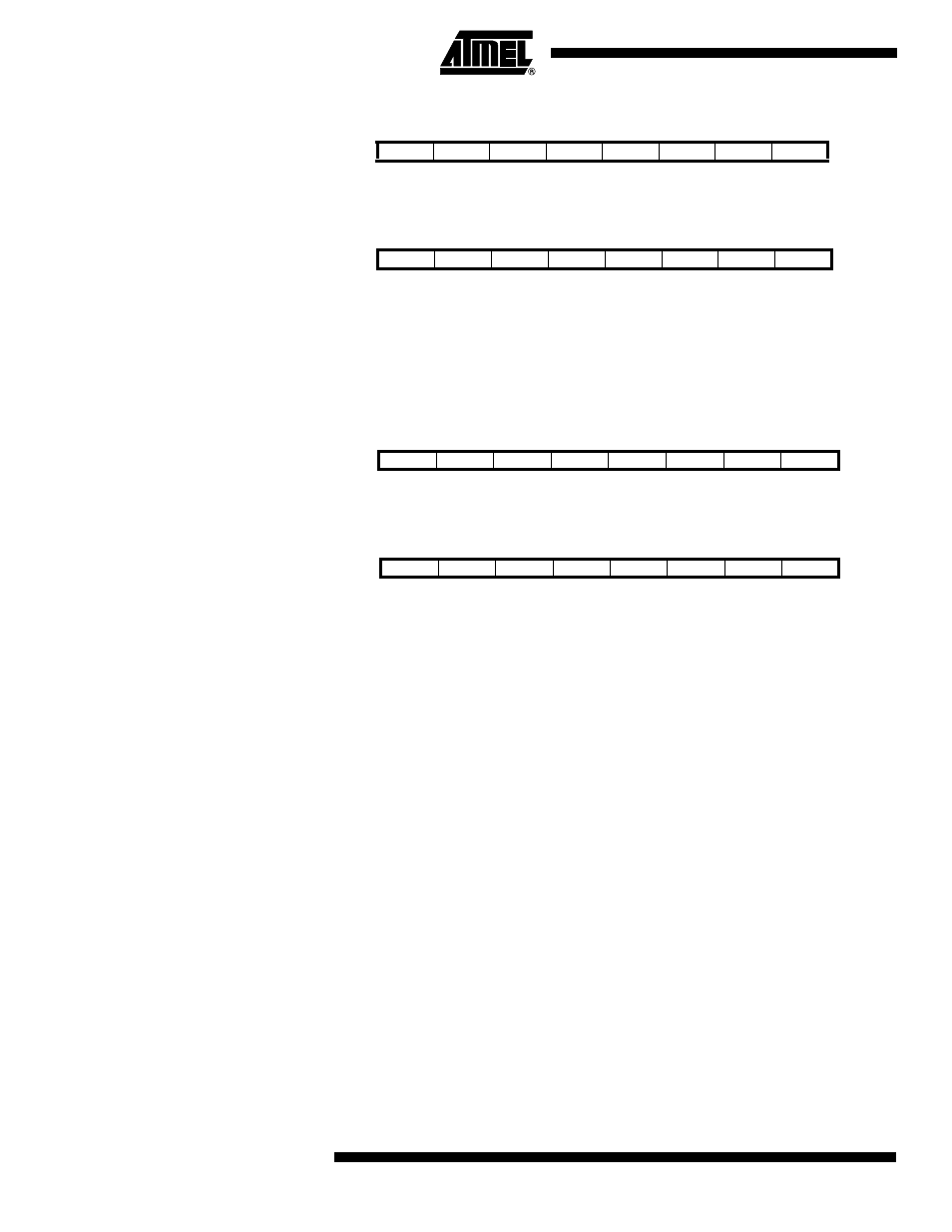
Timer Counter0 – TCNT0
Timer/Counter2 – TCNT2
These 8-bit registers contain the value of the Timer/Counters.
Both Timer/Counters are realized as up or up/down (in PWM mode) counters with read
and write access. If the Timer/Counter is written to and a clock source is selected, it con-
tinues counting in the timer clock cycle following the write operation.
Timer/Counter0 Output
Compare Register – OCR0
Timer/Counter2 Output
Compare Register – OCR2
The Output Compare Registers are 8-bit read/write registers. The Timer/Counter Output
C om p ar e R eg iste rs c on tai n th e d ata to be con tin uo us ly com p ar ed wi th th e
Timer/Counter. Actions on compare matches are specified in TCCR0 and TCCR2. A
software write to the Timer/Counter Register blocks compare matches in the next
Timer/Counter clock cycle. This prevents immediate interrupts when initializing the
Timer/Counter.
A compare match will set the Compare Interrupt Flag in the CPU clock cycle following
the compare event.
Timer/Counters 0 and 2 in
PWM Mode
When PWM mode is selected, the Timer/Counter either wraps (overflows) when it
reaches $FF or it acts as an up/down counter.
If the up/down mode is selected, the Timer/Counter and the Output Compare Registers
(OCR0 or OCR2) form an 8-bit, free-running, glitch-free and phase-correct PWM with
outputs on the PB0(OC0/PWM0) or PB1(OC2/PWM2) pin.
If the Overflow mode is selected, the Timer/Counter and the Output Compare Registers
(OCR0 or OCR2) form an 8-bit, free-running and glitch-free PWM, operating with twice
the speed of the up/down counting mode.
Bit
7
6
5
4
3
2
1
0
$32 ($52)
MSB
LSB
TCNT0
Read/Write
R/W
R/W
R/W
R/W
R/W
R/W
R/W
R/W
Initial Value
0
0
0
0
0
0
0
0
Bit
7
6
5
4
3
2
1
0
$23 ($43)
MSB
LSB
TCNT2
Read/Write
R/W
R/W
R/W
R/W
R/W
R/W
R/W
R/W
Initial Value
0
0
0
0
0
0
0
0
Bit
7
6
5
4
3
2
1
0
$31 ($51)
MSB
LSB
OCR0
Read/Write
R/W
R/W
R/W
R/W
R/W
R/W
R/W
R/W
Initial Value
0
0
0
0
0
0
0
0
Bit
7
6
5
4
3
2
1
0
$22 ($42)
MSB
LSB
OCR2
Read/Write
R/W
R/W
R/W
R/W
R/W
R/W
R/W
R/W
Initial Value
0
0
0
0
0
0
0
0