Timer/counter0 control register – tccr0, Timer/counter2 control register – tccr2, Atmega161(l) – Rainbow Electronics ATmega161L User Manual
Page 42: Bit 3, Table 9. compare mode selec t
42
ATmega161(L)
1228C–AVR–08/02
Timer/Counter0 Control
Register – TCCR0
Timer/Counter2 Control
Register – TCCR2
• Bit 7
–
FOC0/FOC2: Force Output Compare
Writing a logical “1” to this bit forces a change in the compare match output pin PB0
(Timer/Counter0) and PB1 (Timer/Counter2) according to the values already set in
COMn1 and COMn0. If the COMn1 and COMn0 bits are written in the same cycle as
FOC0/FOC2, the new settings will not take effect until the next compare match or
Forced Output Compare Match occurs. The Force Output Compare bit can be used to
change the output pin without waiting for a compare match in the timer. The automatic
action programmed in COMn1 and COMn0 happens as if a Compare Match had
occurred, but no interrupt is generated and the Timer/Counters will not be cleared even
if CTC0/CTC2 is set. The FOC0/FOC2 bits will always be read as zero. The setting of
the FOC0/FOC2 bits has no effect in PWM mode.
• Bit 6
–
PWM0/PWM2: Pulse Width Modulator Enable
When set (one), this bit enables PWM mode for Timer/Counter0 or Timer/Counter2.
This mode is described on page 44.
• Bits 5, 4
–
COM01, COM00/COM21, COM20: Compare Output Mode, Bits 1 and 0
The COMn1 and COMn0 control bits determine any output pin action following a com-
pare match in Timer/Counter0 or Timer/Counter2. Output pin actions affect pins
PB0(OC0) or PB1(OC2). This is an alternative function to an I/O port and the corre-
sponding direction control bit must be set (one) to control an output pin. The control
configuration is shown in Table 9.
Notes:
1. In PWM mode, these bits have a different function. Refer to Table 12 for a detailed
description.
2. n = 0 or 2
• Bit 3
–
CTC0/CTC2: Clear Timer/Counter on Compare Match
When the CTC0 or CTC2 control bit is set (one), Timer/Counter0 or Timer/Counter2 is
reset to $00 in the CPU clock cycle after a compare match. If the control bit is cleared,
the Timer/Counter continues counting and is unaffected by a compare match. When a
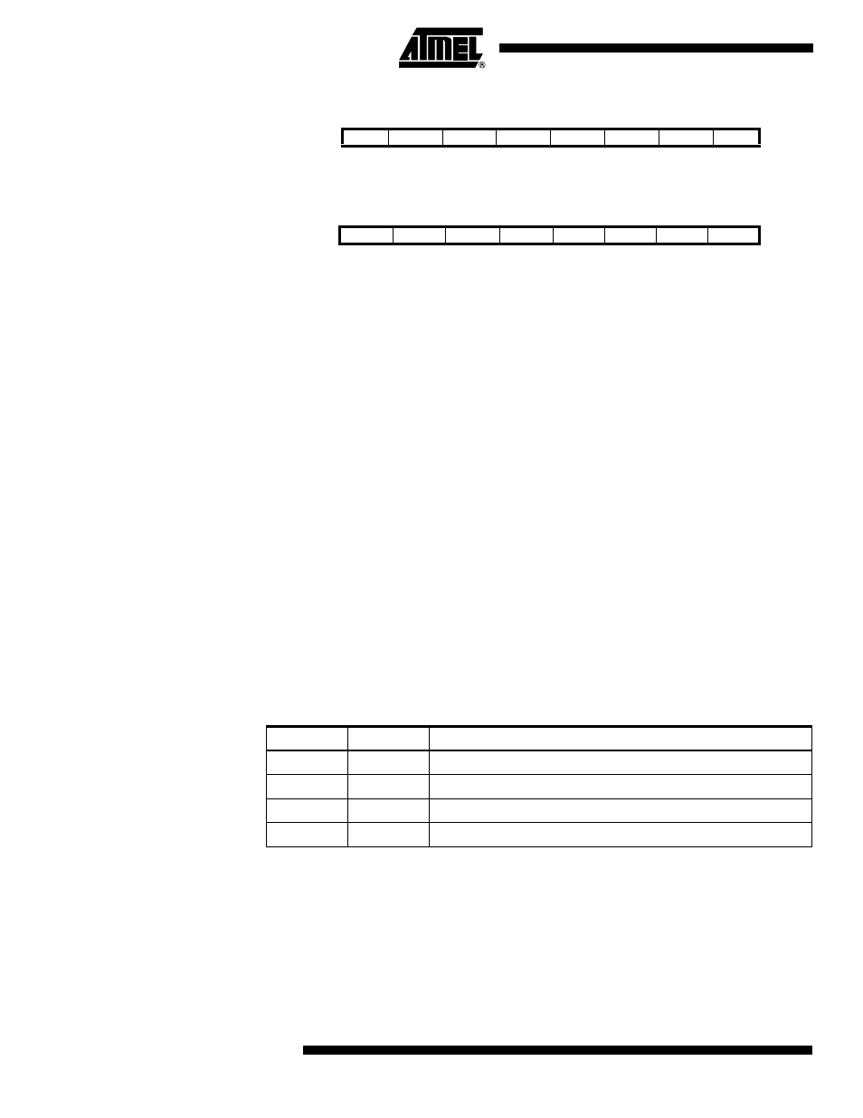
Bit
7
6
5
4
3
2
1
0
$33 ($53)
FOC0
PWM0
COM01
COM00
CTC0
CS02
CS01
CS00
TCCR0
Read/Write
R/W
R/W
R/W
R/W
R/W
R/W
R/W
R/W
Initial Value
0
0
0
0
0
0
0
0
Bit
7
6
5
4
3
2
1
0
$27 ($47)
FOC2
PWM2
COM21
COM20
CTC2
CS22
CS21
CS20
TCCR2
Read/Write
R/W
R/W
R/W
R/W
R/W
R/W
R/W
R/W
Initial Value
0
0
0
0
0
0
0
0
Table 9. Compare Mode Select
(1)(2)
COMn1
COMn0
Description
0
0
Timer/Counter disconnected from output pin OCn.
0
1
Toggle the OCn output line.
1
0
Clear the OCn output line (to zero).
1
1
Set the OCn output line (to one).