Atmega161(l) – Rainbow Electronics ATmega161L User Manual
Page 87
87
ATmega161(L)
1228C–AVR–08/02
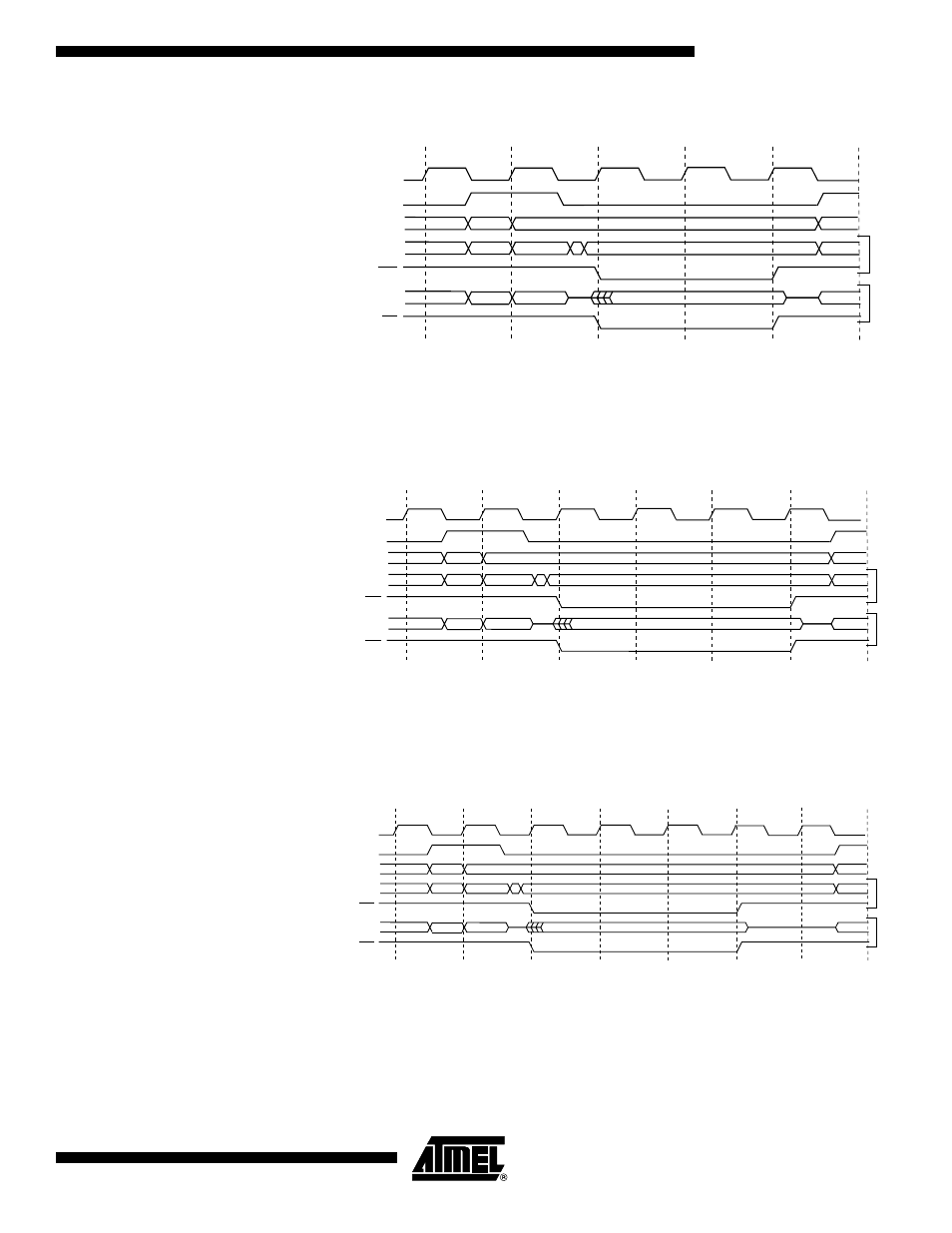
Figure 51. External Data Memory Cycles with SRWn1 = 0 and SRWn0 = 1
(1)
Note:
1. SRWn1 = SRW11 (upper page) or SRW01 (lower page), SRWn0 = SRW10 (upper
page) or SRW00 (lower page). The ALE pulse in period T5 is only present if the next
instruction accesses the RAM (internal or external). The Data and Address will only
change in T5 if ALE is present (the next instruction accesses the RAM).
Figure 52. External Data Memory Cycles with SRWn1 = 1 and SRWn0 = 0
(1)
Note:
1. SRWn1 = SRW11 (upper page) or SRW01 (lower page), SRWn0 = SRW10 (upper
page) or SRW00 (lower page). The ALE pulse in period T6 is only present if the next
instruction accesses the RAM (internal or external). The Data and Address will only
change in T6 if ALE is present (the next instruction accesses the RAM).
Figure 53. External Data Memory Cycles with SRWn1 = 1 and SRWn0 = 1
(1)
Note:
1. SRWn1 = SRW11 (upper page) or SRW01 (lower page), SRWn0 = SRW10 (upper
page) or SRW00 (lower page). The ALE pulse in period T7 is only present if the next
instruction accesses the RAM (internal or external). The Data and Address will only
change in T7 if ALE is present (the next instruction accesses the RAM).
System Clock Ø
ALE
WR
RD
Data/Address [7..0]
Data/Address [7..0]
Address [15..8]
Address
Address
Address
T1
T2
T3
XX
Data
Data
Wr
ite
Read
T5
XX
XX
XX
XX
Prev. addr.
XX
Prev. data
XX
Prev. data
T4
System Clock Ø
ALE
WR
RD
Data/Address [7..0]
Data/Address [7..0]
Address [15..8]
Address
Address
Address
T1
T2
T3
XX
Data
Data
Wr
ite
Read
T6
XX
XX
XX
XX
Prev. addr.
XX
Prev. data
XX
Prev. data
T4
T5
System Clock Ø
ALE
WR
RD
Data/Address [7..0]
Data/Address [7..0]
Address [15..8]
Address
Address
Address
T1
T2
T3
XX
Data
Data
Wr
ite
Read
T7
XX
XX
XX
XX
Prev. addr.
XX
Prev. data
XX
Prev. data
T4
T5
T6