Alternate functions of port g, Atmega128(l) – Rainbow Electronics ATmega128L User Manual
Page 80
80
ATmega128(L)
2467B–09/01
Alternate Functions of Port G
In ATmega103 compatibility mode, only the alternate functions are the defaults for Port
G, and Port G cannot be used as General Digital Port Pins. The alternate pin configura-
tion is as follows:
• TOSC1 - Port G, Bit 4
TOSC2, Timer Oscillator pin 1: When the AS0 bit in ASSR is set (one) to enable asyn-
chronous clocking of Timer/Counter0, pin PG4 is disconnected from the port, and
becomes the inverting output of the oscillator amplifier. In this mode, a crystal oscillator
is connected to this pin, and the pin can not be used as an I/O pin.
• TOSC2 - Port G, Bit 3
TOSC2, Timer Oscillator pin 2: When the AS0 bit in ASSR is set (one) to enable asyn-
chronous clocking of Timer/Counter0, pin PG3 is disconnected from the port, and
becomes the input of the inverting oscillator amplifier. In this mode, a crystal oscillator is
connected to this pin, and the pin can not be used as an I/O pin.
• ALE - Port G, Bit 2
ALE is the external data memory Address Latch Enable signal.
• RD - Port G, Bit 1
RD is the external data memory read control strobe.
• WR - Port G, Bit 0
WR is the external data memory write control strobe.
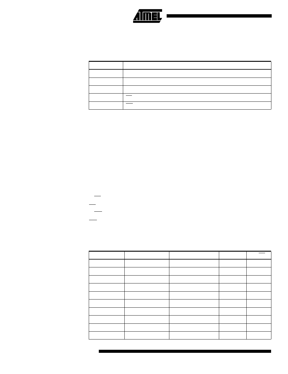
Table 46 and Table 47 relates the alternate functions of Port G to the overriding signals
shown in
Table 45. Port G Pins Alternate Functions
Port Pin
Alternate Function
PG4
TOSC1 (RTC oscillator Timer/Counter 0)
PG3
TOSC2 (RTC oscillator Timer/Counter 0)
PG2
ALE (Address Latch Enable to external memory)
PG1
RD (Read strobe to external memory)
PG0
WR (Write strobe to external memory)
Table 46. Overriding Signals for Alternate Functions in PG4..PG1
Signal Name
PG4/TOSC1
PG3/TOSC2
PG2/ALE
PG1/RD
PUOE
AS0
AS0
SRE
SRE
PUOV
0
0
0
0
DDOE
AS0
AS0
SRE
SRE
DDOV
0
0
1
1
PVOE
0
0
SRE
SRE
PVOV
0
0
ALE
RD
DIEOE
AS0
AS0
0
0
DIEOV
0
0
0
0
DI
–
–
–
–
AIO
T/C0 OSC INPUT
T/C0 OSC OUTPUT
–
–