Alternate functions of port e, Atmega128(l) – Rainbow Electronics ATmega128L User Manual
Page 76
76
ATmega128(L)
2467B–09/01
Alternate Functions of Port E
The Port E pins with alternate functions are shown in
Note:
1. IC3, T3, OC3C, OC3B, OC3B, OC3A, and XCK0 not applicable in ATmega103 com-
patibility mode.
• INT7/IC3 - Port E, Bit 7
INT7, External Interrupt source 7: The PE7 pin can serve as an external interrupt
source.
IC3 - Inp ut Cap ture P in 3: The P E 7 p in c an a c t a s an i np ut c apt ure pin for
Timer/Counter3.
• INT6/T3 - Port E, Bit 6
INT6, External Interrupt source 6: The PE6 pin can serve as an external interrupt
source.
T3, Timer/Counter3 counter source.
• INT5/OC3C - Port E, Bit 5
INT5, External Interrupt source 5: The PE5 pin can serve as an external interrupt
source.
OC3C, Output Compare matchC output: The PE5 pin can serve as an external output
for the Timer/Counter3 output compareC. The pin has to be configured as an output
(DDE5 set “one”) to serve this function. The OC3C pin is also the output pin for the
PWM mode timer function.
• INT4/OC3B - Port E, Bit 4
INT4, External Interrupt source 4: The PE4 pin can serve as an external interrupt
source.
OC3B, Output Compare matchB output: The PE4 pin can serve as an external output
for the Timer/Counter3 output compareB. The pin has to be configured as an output
(DDE4 set (one)) to serve this function. The OC3B pin is also the output pin for the PWM
mode timer function.
• AIN1/OC3A - Port E, Bit 3
AIN1 - Analog Comparator Negative Input. This pin is directly connected to the negative
input of the analog comparator.
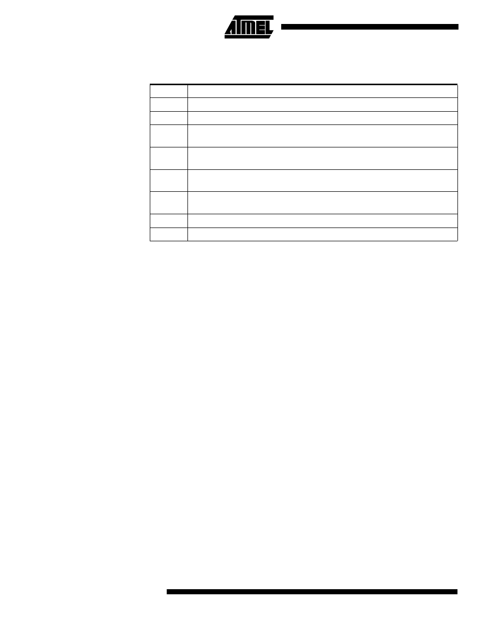
Table 39. Port E Pins Alternate Functions
Port Pin
Alternate Function
PE7
INT7/IC3
(External Interrupt7 Input or Timer/Counter3 Input Capture Trigger)
PE6
INT6/ T3
(External Interrupt6 Input or Timer/Counter3 Clock Input)
PE5
INT5/OC3C
(External Interrupt5 Input or Output Compare and PWM Output C for
Timer/Counter3)
PE4
INT4/OC3B
(External Interrupt4 Input or Output Compare and PWM Output B for
Timer/Counter3)
PE3
AIN1/OC3A
(Analog Comparator Negative Input or Output Compare and PWM
Output A for Timer/Counter3)
PE2
AIN0/XCK0
(Analog Comparator Positive Input or USART0 external clock
input/output)
PE1
PDO/TXD0 (Programming Data Output or UART0 Transmit Pin)
PE0
PDI/RXD0 (Programming Data Input or UART0 Receive Pin)