Timer/counter timing diagrams, Atmega128(l) – Rainbow Electronics ATmega128L User Manual
Page 125
125
ATmega128(L)
2467B–09/01
decrements. The PWM frequency for the output when using phase and frequency
correct PWM can be calculated by the following equation:
The N variable represents the prescaler divider (1, 8, 64, 256, or 1024).
The extreme values for the OCRnx register represent special cases when generating a
PWM waveform output in the phase correct PWM mode. If the OCRnx is set equal to
BOTTOM the output will be continuously low and if set equal to TOP the output will be
set to high for non-inverted PWM mode. For inverted PWM the output will have the
opposite logic values.
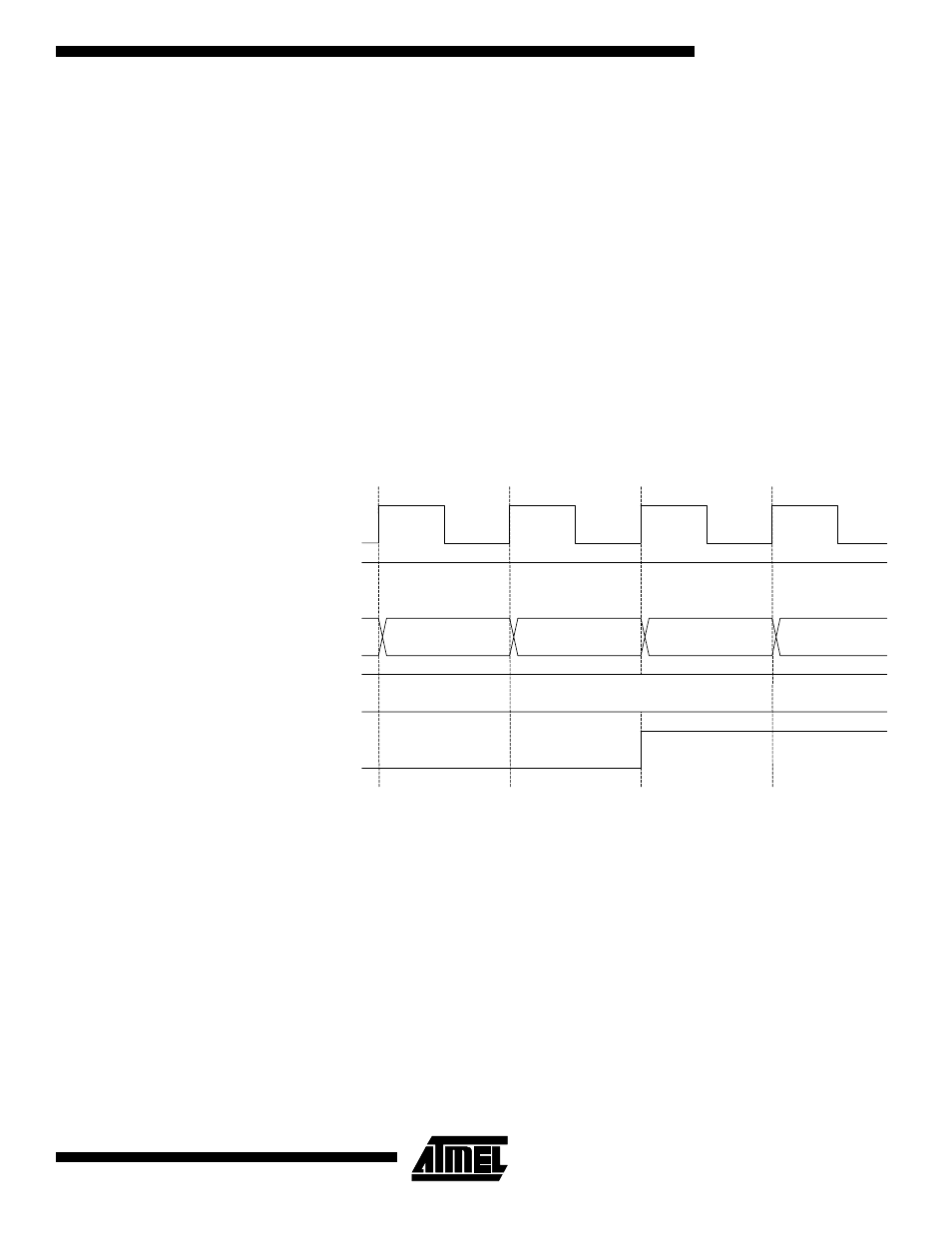
Timer/Counter Timing
Diagrams
The Timer/Counter is a synchronous design and the timer clock (clk
Tn
) is therefore
shown as a clock enable signal in the following figures. The figures include information
on when interrupt flags are set, and when the OCRnx register is updated with the
OCRnx buffer value (only for modes utilizing double buffering).
Figure 54 shows a timing
diagram for the setting of OCFnx.
Figure 54. Timer/Counter Timing Diagram, Setting of OCFnx, no Prescaling
Figure 55 shows the same timing data, but with the prescaler enabled.
f
OCn xPFC PWM
f
clk_I/O
2 N TOP
⋅ ⋅
----------------------------
=
clk
Tn
(clk
I/O
/1)
OCFnx
clk
I/O
OCRnx
TCNTn
OCRnx Value
OCRnx - 1
OCRnx
OCRnx + 1
OCRnx + 2