D table 121. pi, Table 123, Table 124 – Rainbow Electronics ATmega128L User Manual
Page 283: Atmega128(l)
283
ATmega128(L)
2467B–09/01
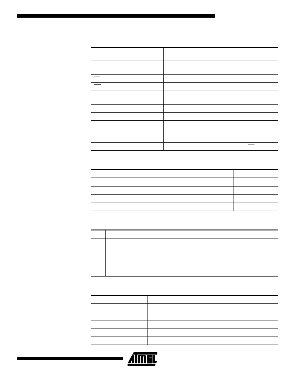
Table 121. Pin Name Mapping
Signal Name in
Programming Mode
Pin Name
I/O
Function
RDY/BSY
PD1
O
0: Device is busy programming, 1: Device is ready
for new command
OE
PD2
I
Output Enable (Active low)
WR
PD3
I
Write Pulse (Active low)
BS1
PD4
I
Byte Select 1 (“0” selects low byte, “1” selects high
byte)
XA0
PD5
I
XTAL Action Bit 0
XA1
PD6
I
XTAL Action Bit 1
PAGEL
PD7
I
Program Memory and EEPROM data Page Load
BS2
PA0
I
Byte Select 2 (“0” selects low byte, “1” selects 2’nd
high byte)
DATA
PB7-0
I/O
Bidirectional Data bus (Output when OE is low)
Table 122. Pin Values Used to Enter Programming Mode
Pin
Symbol
Value
PAGEL
Prog_enable[3]
0
XA1
Prog_enable[2]
0
XA0
Prog_enable[1]
0
BS1
Prog_enable[0]
0
Table 123. XA1 and XA0 Coding
XA1
XA0
Action when XTAL1 is Pulsed
0
0
Load Flash or EEPROM Address (High or low address byte determined by
BS1)
0
1
Load Data (High or Low data byte for Flash determined by BS1)
1
0
Load Command
1
1
No Action, Idle
Table 124. Command Byte Bit Coding
Command Byte
Command Executed
1000 0000
Chip Erase
0100 0000
Write Fuse Bits
0010 0000
Write Lock Bits
0001 0000
Write Flash
0001 0001
Write EEPROM