Scanning the digital port pins, Atmega128(l) – Rainbow Electronics ATmega128L User Manual
Page 248
248
ATmega128(L)
2467B–09/01
Scanning the Digital Port Pins
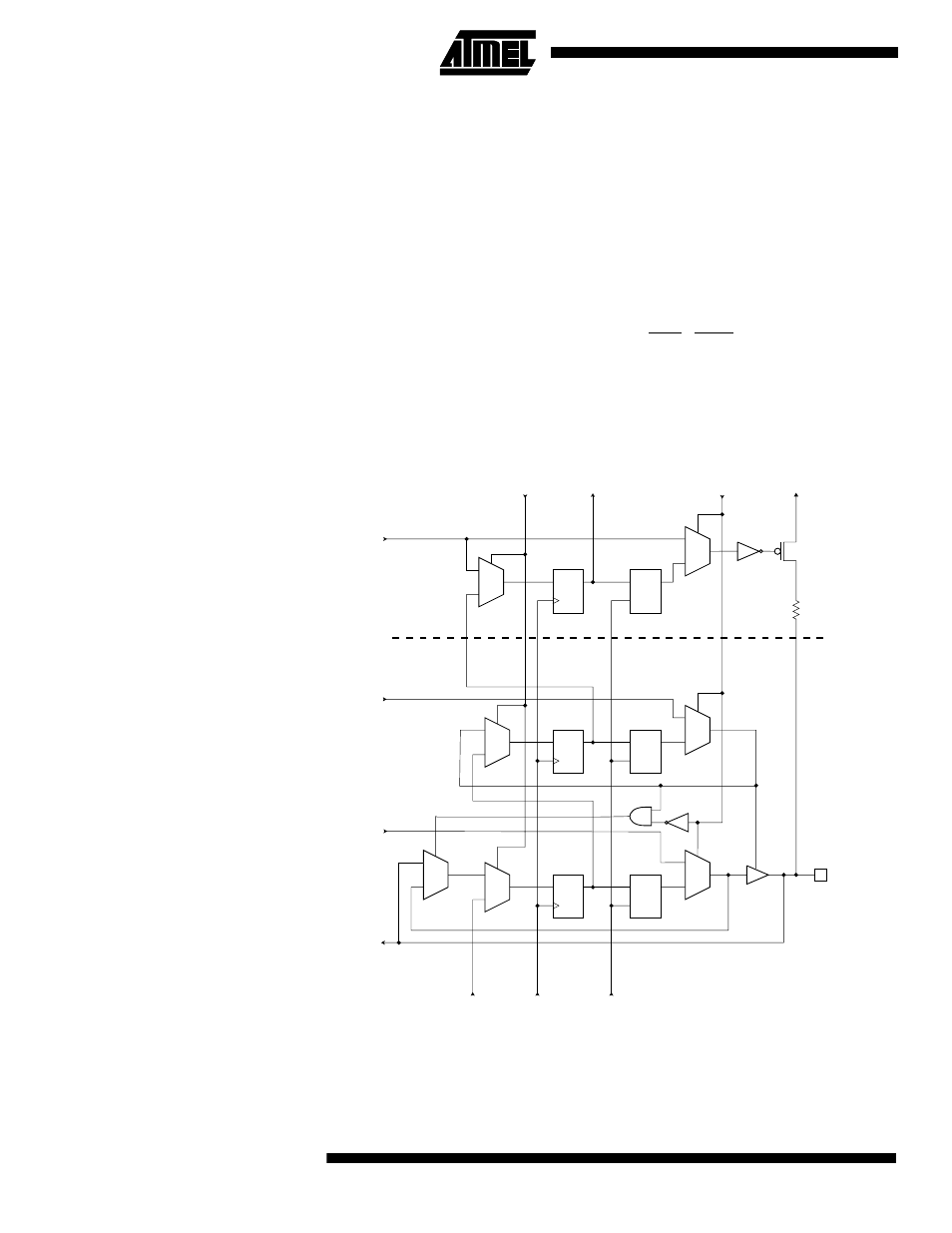
Figure 123 shows the Boundary-scan Cell for a bidirectional port pin with pull-up func-
tion. The cell consists of a standard Boundary-scan cell for the Pull-up Enable – PUExn
– function, and a bidirectional pin cell that combines the three signals Output Control –
OCxn, Output Data – ODxn, and Input Data – IDxn, into only a two-stage shift register.
The port and pin indexes are not used in the following description
The Boundary-scan logic is not included in the figures in the Data Sheet.
shows a simple digital Port Pin as described in the section
Figure 123 replaces the dashed box in Figure 124.
When no alternate port function is present, the Input Data – ID corresponds to the PINxn
register value (but ID has no synchronizer), Output Data corresponds to the PORT reg-
ister, Output Control corresponds to the Data Direction – DD register, and the Pull-up
Enable – PUExn – corresponds to logic expression PUD · DDxn · PORTxn.
Digital alternate port functions are connected outside the dotted box in
Figure 124 to
make the scan chain read the actual pin value. For Analog function, there is a direct
connection from the external pin to the analog circuit, and a scan chain is inserted on
the interface between the digital logic and the analog circuitry.
Figure 123. Boundary-scan Cell for Bidirectional Port Pin with Pull-Up Function.
D
Q
D
Q
G
0
1
0
1
D
Q
D
Q
G
0
1
0
1
0
1
0
1
D
Q
D
Q
G
0
1
Port Pin (PXn)
Vcc
EXTEST
To Next Cell
ShiftDR
Output Control (OC)
Pullup Enable (PUE)
Output Data (OD)
Input Data (ID)
From Last Cell
UpdateDR
ClockDR
FF2
LD2
FF1
LD1
LD0
FF0