Address latch requirements, Pull-up and bus-keeper, Atmega128(l) – Rainbow Electronics ATmega128L User Manual
Page 26
26
ATmega128(L)
2467B–09/01
The control bits for the External Memory Interface are located in three registers, the
MCU Control Register – MCUCR, the External Memory Control Register A – XMCRA,
and the External Memory Control Register B – XMCRB.
When the XMEM interface is enabled, the XMEM interface will override the setting in the
data direction registers that corresponds to the ports dedicated to the XMEM interface.
For details about the port override, see the alternate functions in section
page 60. The XMEM interface will auto-detect whether an access is internal or external.
If the access is external, the XMEM interface will output address, data, and the control
signals on the ports according to
Figure 13 (this figure shows the wave forms without
wait-states). When ALE goes from high-to-low, there is a valid address on AD7:0. ALE is
low during a data transfer. When the XMEM interface is enabled, also an internal access
will cause activity on address, data and ALE ports, but the RD and WR strobes will not
toggle during internal access. When the External Memory Interface is disabled, the nor-
mal pin and data direction settings are used. Note that when the XMEM interface is
disabled, the address space above the internal SRAM boundary is not mapped into the
internal SRAM.
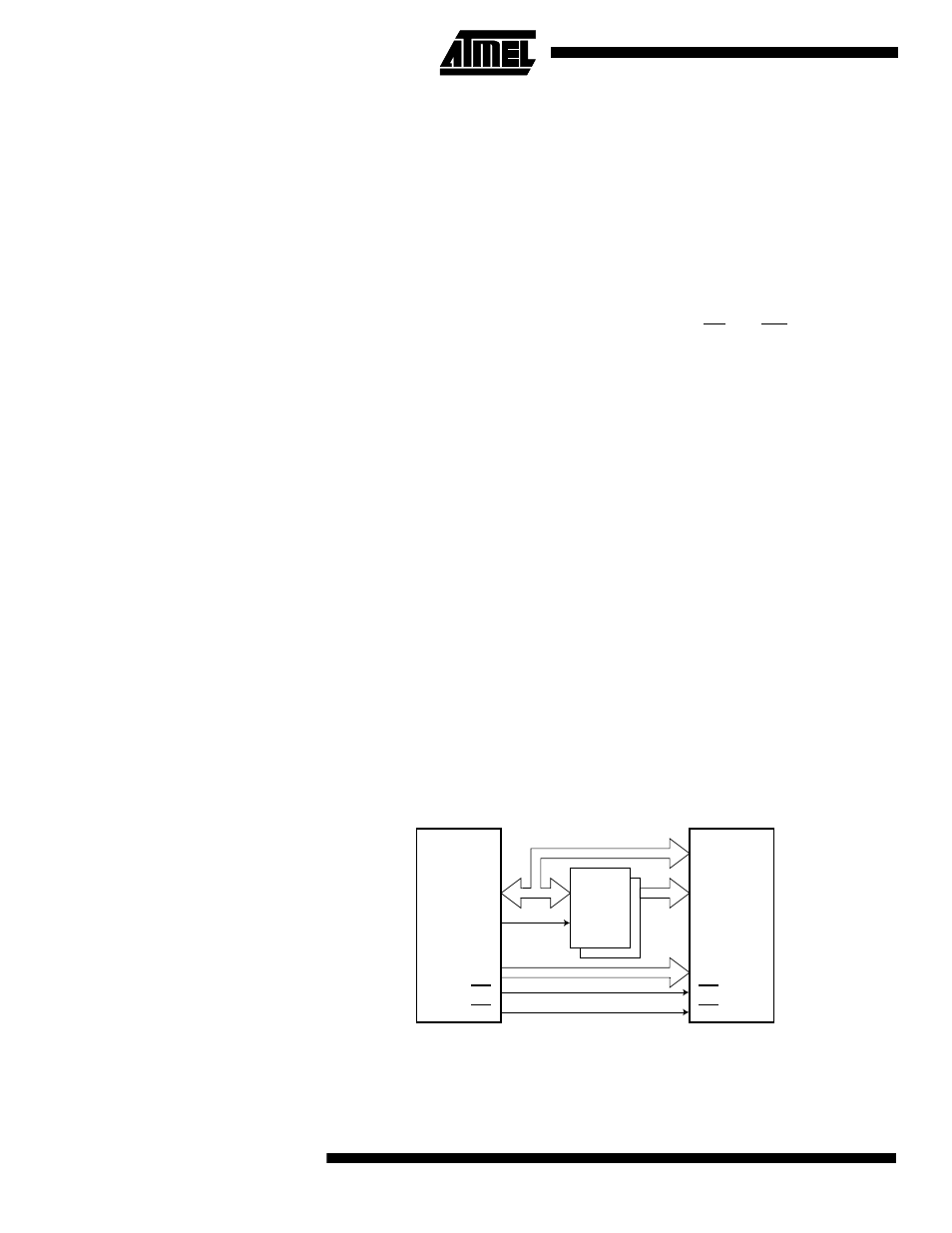
Figure 12 illustrates how to connect an external SRAM to the AVR using
an octal latch (typically “74 x 573” or equivalent) which is transparent when G is high.
Address Latch Requirements
Due to the high-speed operation of the XRAM interface, the address latch must be
selected with care for system frequencies above 8 MHz @ 4V and 4 MHz @ 2.7V.
When operating at conditions above these frequencies, the typical old style 74HC series
latch becomes inadequate. The external memory interface is designed in compliance to
the 74AHC series latch. However, most latches can be used as long they comply with
the main timing parameters. The main parameters for the address latch are:
•
D to Q propagation delay (t
PD
).
•
Data setup time before G low (t
SU
).
•
Data (address) hold time after G low (
TH
).
The external memory interface is designed to guaranty minimum address hold time after
G is asserted low of t
h
= 5 ns. Refer to t
LAXX_LD
/t
LLAXX_ST
Tables 138 through Tables 145 on pages 317 - 319. The D-to-Q propagation delay
(t
PD
) must be taken into consideration when calculating the access time requirement of
the external component. The data setup time before G low (t
SU
) must not exceed
address valid to ALE low (t
AVLLC
) minus PCB wiring delay (dependent on the capacitive
load).
Figure 12. External SRAM Connected to the AVR
Pull-up and Bus-keeper
The pull-ups on the AD7:0 ports may be activated if the corresponding Port register is
written to one. To reduce power consumption in sleep mode, it is recommended to dis-
able the pull-ups by writing the Port register to zero before entering sleep.
D[7:0]
A[7:0]
A[15:8]
RD
WR
SRAM
D
Q
G
AD7:0
ALE
A15:8
RD
WR
AVR