Timer/counter interrupt mask register – timsk, Timer/counter interrupt flag register – tifr, Atmega128(l) – Rainbow Electronics ATmega128L User Manual
Page 103
103
ATmega128(L)
2467B–09/01
read as the previous value (before entering sleep) until the next rising TOSC1 edge.
The phase of the TOSC clock after waking up from Power-save mode is essentially
unpredictable, as it depends on the wake-up time. The recommended procedure for
reading TCNT0 is thus as follows:
1.
Write any value to either of the registers OCR0 or TCCR0.
2.
Wait for the corresponding Update Busy Flag to be cleared.
3.
Read TCNT0.
•
During asynchronous operation, the synchronization of the interrupt flags for the
asynchronous timer takes 3 processor cycles plus one timer cycle. The timer is
therefore advanced by at least one before the processor can read the timer value
causing the setting of the interrupt flag. The output compare pin is changed on the
timer clock and is not synchronized to the processor clock.
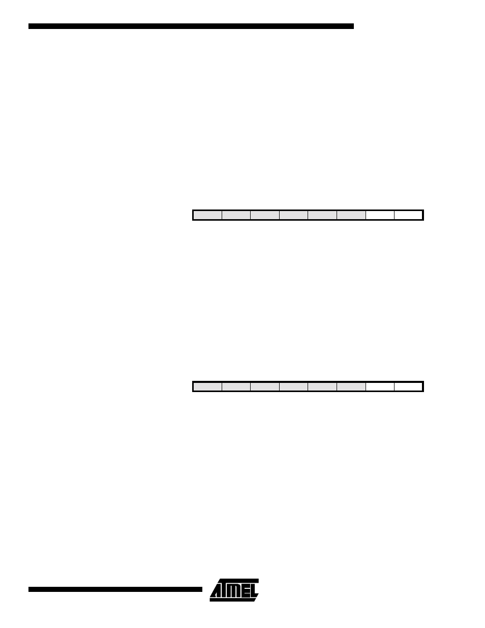
Timer/Counter Interrupt Mask
Register – TIMSK
• Bit 1 - OCIE0: Timer/Counter0 Output Compare Match Interrupt Enable
When the OCIE0 bit is written to one, and the I-bit in the Status Register is set (one), the
Timer/Counter0 Compare Match interrupt is enabled. The corresponding interrupt is
executed if a compare match in Timer/Counter0 occurs, i.e. when the OCF0 bit is set in
the Timer/Counter Interrupt Flag Register – TIFR.
• Bit 0 - TOIE0: Timer/Counter0 Overflow Interrupt Enable
When the TOIE0 bit is written to one, and the I-bit in the Status Register is set (one), the
Timer/Counter0 Overflow interrupt is enabled. The corresponding interrupt is executed if
an overflow in Timer/Counter0 occurs, i.e. when the TOV0 bit is set in the Timer/Counter
Interrupt Flag Register – TIFR.
Timer/Counter Interrupt Flag
Register – TIFR
• Bit 1 - OCF0: Output Compare Flag 0
The OCF0 bit is set (one) when a compare match occurs between the Timer/Counter0
and the data in OCR0 – Output Compare Register0. OCF0 is cleared by hardware when
executing the corresponding interrupt handling vector. Alternatively, OCF0 is cleared by
writing a logic one to the flag. When the I-bit in SREG, OCIE0 (Timer/Counter0 Com-
pare match Interrupt Enable), and OCF0 are set (one), the Timer/Counter0 Compare
match Interrupt is executed.
• Bit 0 - TOV0: Timer/Counter0 Overflow Flag
The bit TOV0 is set (one) when an overflow occurs in Timer/Counter0. TOV0 is cleared
by hardware when executing the corresponding interrupt handling vector. Alternatively,
TOV0 is cleared by writing a logic one to the flag. When the SREG I-bit, TOIE0
(Ti m e r/ Co u nt e r0 O ver flo w I nt e rru p t E n ab l e ), a n d TOV 0 ar e s e t ( on e ), t h e
Timer/Counter0 Overflow interrupt is executed. In PWM mode, this bit is set when
Timer/Counter0 changes counting direction at $00.
Bit
7
6
5
4
3
2
1
0
OCIE2
TOIE2
TICIE1
OCIE1A
OCIE1B
TOIE1
OCIE0
TOIE0
TIMSK
Read/Write
R/W
R/W
R/W
R/W
R/W
R/W
R/W
R/W
Initial value
0
0
0
0
0
0
0
0
Bit
7
6
5
4
3
2
1
0
OCF2
TOV2
ICF1
OCF1A
OCF1B
TOV1
OCF0
TOV0
TIFR
Read/Write
R/W
R/W
R/W
R/W
R/W
R/W
R/W
R/W
Initial value
0
0
0
0
0
0
0
0