Definitions, Timer/counter clock sources, Atmega162/v – Rainbow Electronics ATmega162V User Manual
Page 89
89
ATmega162/V
2513E–AVR–09/03
inactive when no clock source is selected. The output from the clock select logic is
referred to as the timer clock (clk
T
0).
The double buffered Output Compare Register (OCR0) is compared with the
Timer/Counter value at all times. The result of the compare can be used by the Wave-
form Generator to generate a PWM or variable frequency output on the Output Compare
pin (OC0). See “Output Compare Unit” on page 90. for details. The Compare Match
event will also set the Compare Flag (OCF0) which can be used to generate an output
compare interrupt request.
Definitions
Many register and bit references in this section are written in general form. A lower case
“n” replaces the Timer/Counter number, in this case 0. However, when using the register
or bit defines in a program, the precise form must be used i.e., TCNT0 for accessing
Timer/Counter0 counter value and so on.
The definitions in Table 46 are also used extensively throughout the document.
Timer/Counter Clock
Sources
The Timer/Counter can be clocked by an internal or an external clock source. The clock
source is selected by the Clock Select logic which is controlled by the Clock Select
(CS02:0) bits located in the Timer/Counter Control Register (TCCR0). For details on
c l o c k s o u r c e s a n d p r e s c a l e r , s e e “ T i m e r /C o u n te r 0 , T i m e r / C o u n t e r 1 , a n d
Timer/Counter3 Prescalers” on page 103.
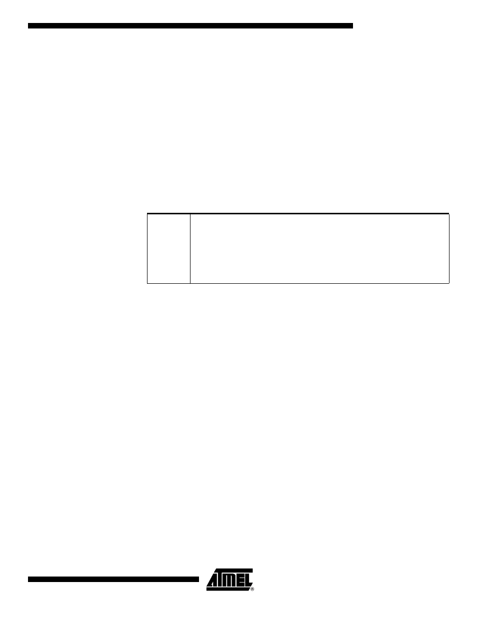
Table 46. Definitions
BOTTOM
The counter reaches the BOTTOM when it becomes 0x00.
MAX
The counter reaches its MAXimum when it becomes 0xFF (decimal 255).
TOP
The counter reaches the TOP when it becomes equal to the highest
value in the count sequence. The TOP value can be assigned to be the
fixed value 0xFF (MAX) or the value stored in the OCR0 Register. The
assignment is dependent on the mode of operation.