Pin change mask register 1 – pcmsk1, Pin change mask register 0 – pcmsk0, Atmega162/v – Rainbow Electronics ATmega162V User Manual
Page 87
87
ATmega162/V
2513E–AVR–09/03
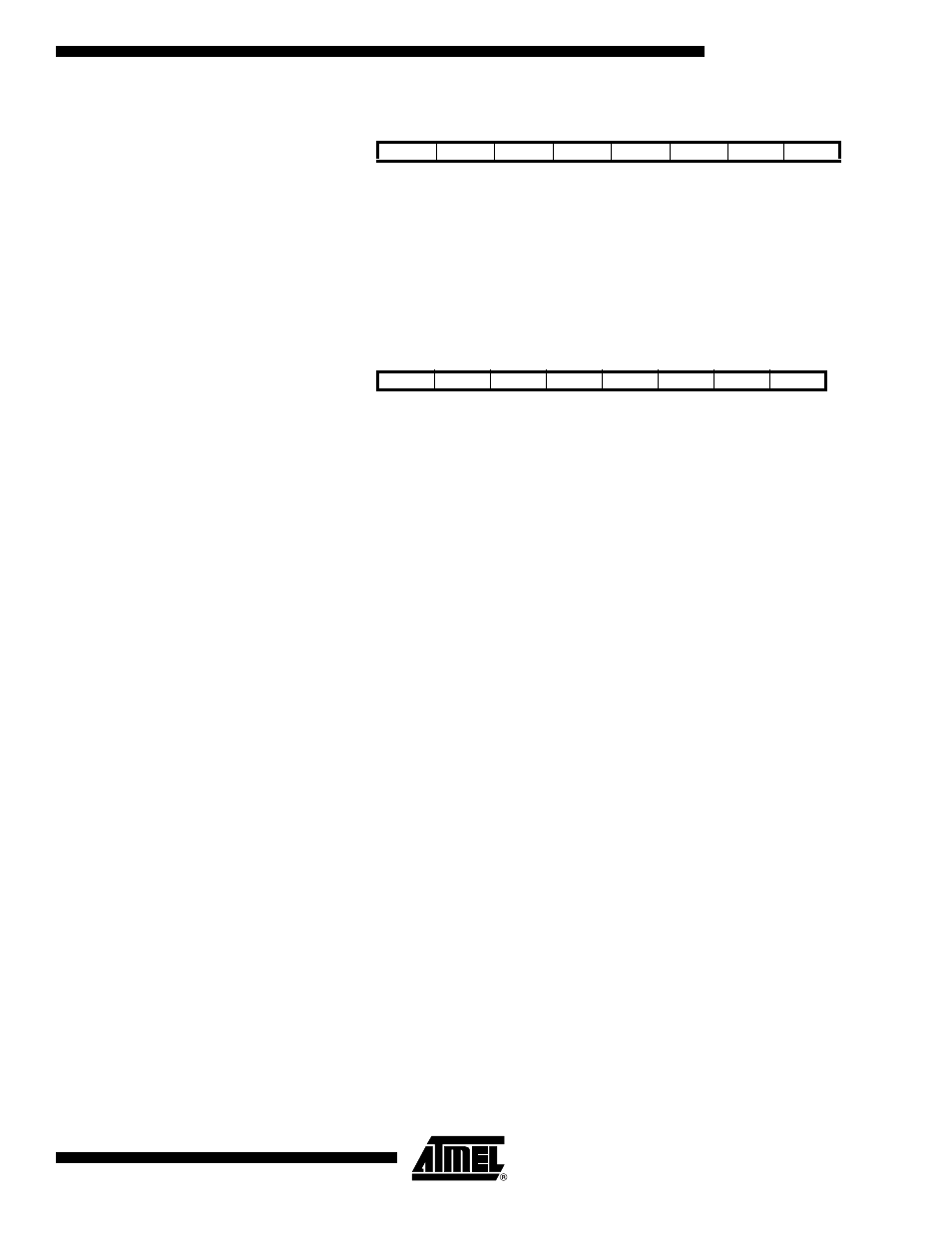
Pin Change Mask Register 1 –
PCMSK1
• Bit 7..0 – PCINT15..8: Pin Change Enable Mask 15..8
Each PCINT15..8 bit selects whether pin change interrupt is enabled on the correspond-
ing I/O pin. If PCINT15..8 is set and the PCIE1 bit in GICR is set, pin change interrupt is
enabled on the corresponding I/O pin. If PCINT15..8 is cleared, pin change interrupt on
the corresponding I/O pin is disabled.
Pin Change Mask Register 0 –
PCMSK0
• Bit 7..0 – PCINT7..0: Pin Change Enable Mask 7..0
Each PCINT7..0 bit selects whether pin change interrupt is enabled on the correspond-
ing I/O pin. If PCINT7..0 is set and the PCIE0 bit in GICR is set, pin change interrupt is
enabled on the corresponding I/O pin. If PCINT7..0 is cleared, pin change interrupt on
the corresponding I/O pin is disabled.
The mapping between I/O pins and PCINT bits can be found in Figure 1 on page 2. Note
that the Pin Change Mask Register are located in Extended I/O. Thus, the pin change
interrupts are not supported in ATmega161 compatibility mode.
Bit
7
6
5
4
3
2
1
0
PCINT15
PCINT14
PCINT13
PCINT12
PCINT11
PCINT10
PCINT9
PCINT9
PCMSK1
Read/Write
R/W
R/W
R/W
R/W
R/W
R/W
R/W
R/W
Initial Value
0
0
0
0
0
0
0
0
Bit
7
6
5
4
3
2
1
0
PCINT7
PCINT6
PCINT5
PCINT4
PCINT3
PCINT2
PCINT1
PCINT0
PCMSK0
Read/Write
R/W
R/W
R/W
R/W
R/W
R/W
R/W
R/W
Initial Value
0
0
0
0
0
0
0
0