Atmega162 boundary- scan order, Atmega162/v – Rainbow Electronics ATmega162V User Manual
Page 212
212
ATmega162/V
2513E–AVR–09/03
ATmega162 Boundary-
scan Order
Table 88 shows the Scan order between TDI and TDO when the Boundary-scan chain
is selected as data path. Bit 0 is the LSB; the first bit scanned in, and the first bit
scanned out. The scan order follows the pinout order as far as possible. Therefore, the
bits of Port A and Port E is scanned in the opposite bit order of the other ports. Excep-
tions from the rules are the Scan chains for the analog circuits, which constitute the
most significant bits of the scan chain regardless of which physical pin they are con-
nected to. In Figure 87, PXn. Data corresponds to FF0, PXn. Control corresponds to
FF1, and PXn. Pullup_enable corresponds to FF2. Bit 4, 5, 6, and 7of Port C is not in the
scan chain, since these pins constitute the TAP pins when the JTAG is enabled.
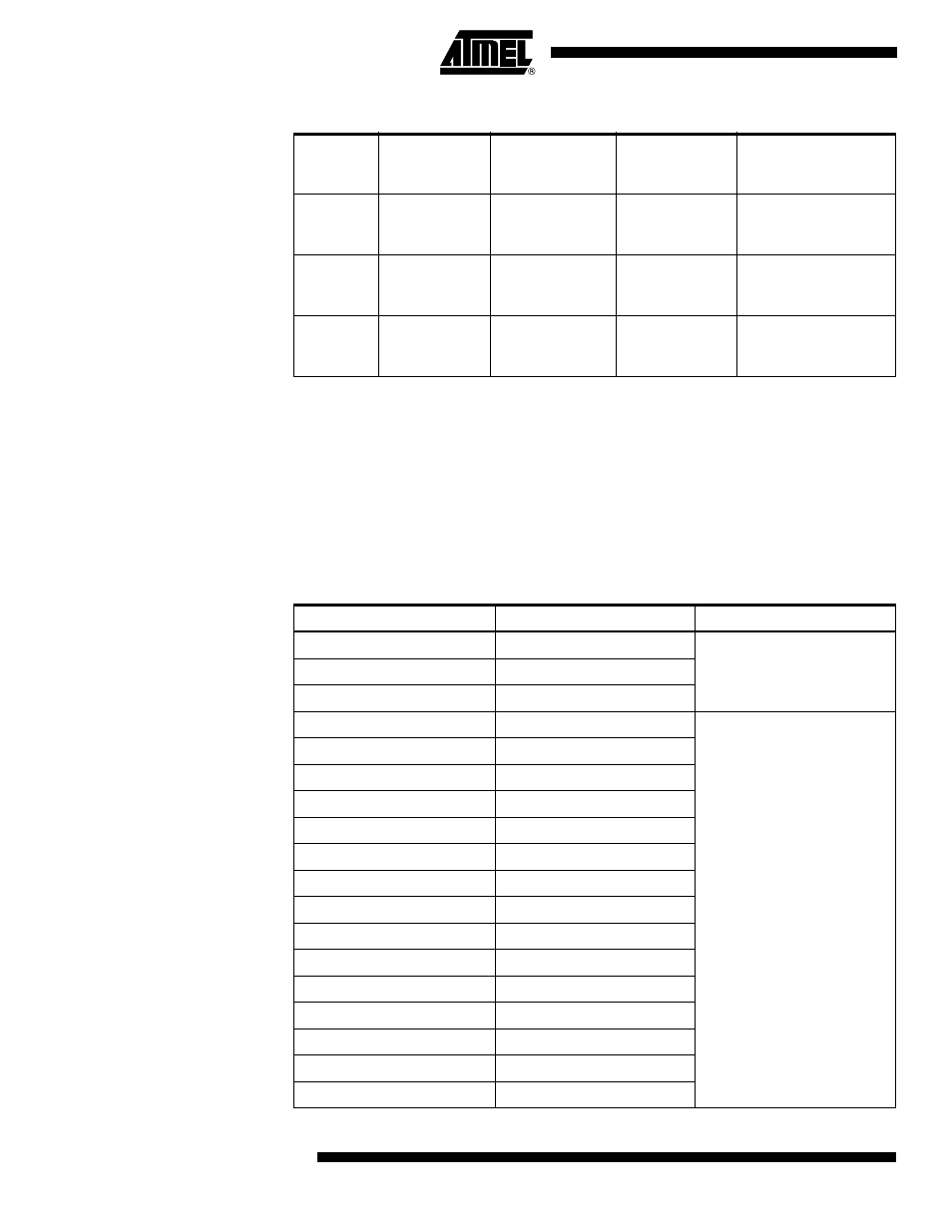
Table 87. Boundary-scan Signals for the Analog Comparator
Signal
Name
Direction as
seen from the
Comparator
Description
Recommended
Input when Not
in Use
Output Values when
Recommended
Inputs are Used
AC_IDLE
input
Turns off Analog
comparator
when true
1
Depends upon µC
code being executed
ACO
output
Analog
Comparator
Output
Will become
input to µC code
being executed
0
ACBG
input
Bandgap
Reference
enable
0
Depends upon µC
code being executed
Table 88. ATmega162 Boundary-scan Order
Bit Number
Signal Name
Module
105
AC_IDLE
Comparator
104
ACO
103
ACBG
102
PB0.Data
Port B
101
PB0.Control
100
PB0.Pullup_Enable
99
PB1.Data
98
PB1.Control
97
PB1.Pullup_Enable
96
PB2.Data
95
PB2.Control
94
PB2.Pullup_Enable
93
PB3.Data
92
PB3.Control
91
PB3.Pullup_Enable
90
PB4.Data
89
PB4.Control
88
PB4.Pullup_Enable