Pull-up and bus keeper, Timing, Figure 13 – Rainbow Electronics ATmega162V User Manual
Page 26: Atmega162/v
26
ATmega162/V
2513E–AVR–09/03
Pull-up and Bus Keeper
The pull-up resistors on the AD7:0 ports may be activated if the corresponding Port reg-
ister is written to one. To reduce power consumption in sleep mode, it is recommended
to disable the pull-ups by writing the Port register to zero before entering sleep.
The XMEM interface also provides a bus keeper on the AD7:0 lines. The Bus Keeper
can be disabled and enabled in software as described in “Special Function IO Register –
SFIOR” on page 30. When enabled, the Bus Keeper will keep the previous value on the
AD7:0 bus while these lines are tri-stated by the XMEM interface.
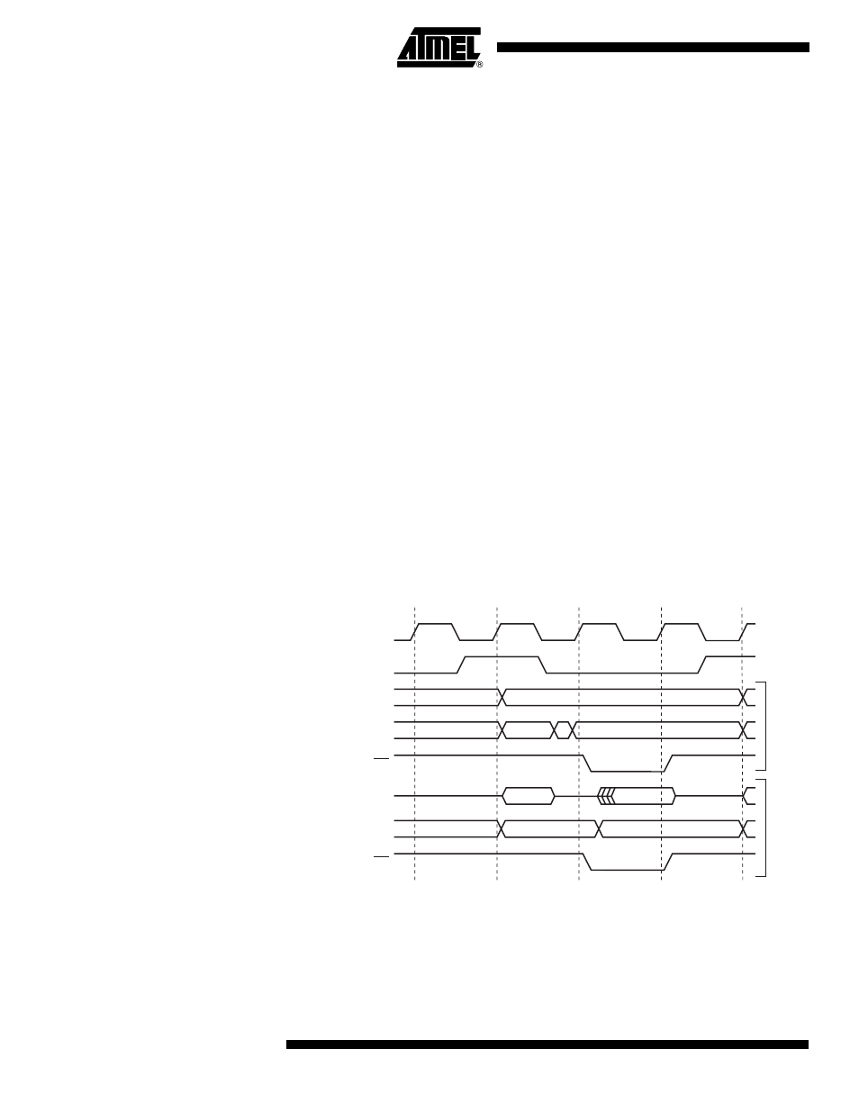
Timing
External memory devices have various timing requirements. To meet these require-
ments, the ATmega162 XMEM interface provides four different wait-states as shown in
Table 3. It is important to consider the timing specification of the external memory
device before selecting the wait-state. The most important parameters are the access
time for the external memory in conjunction with the set-up requirement of the
ATmega162. The access time for the external memory is defined to be the time from
receiving the chip select/address until the data of this address actually is driven on the
bus. The access time cannot exceed the time from the ALE pulse is asserted low until
data must be stable during a read sequence (t
LLRL
+ t
RLRH
- t
DVRH
122 on page 271). The different wait-states are set up in software. As an additional fea-
ture, it is possible to divide the external memory space in two sectors with individual
wait-state settings. This makes it possible to connect two different memory devices with
different timing requirements to the same XMEM interface. For XMEM interface timing
details, please refer to Figure 118 to Figure 121, and Table 115 to Table 122.
Note that the XMEM interface is asynchronous and that the waveforms in the figures
below are related to the internal system clock. The skew between the internal and exter-
nal clock (XTAL1) is not guaranteed (it varies between devices, temperature, and supply
voltage). Consequently, the XMEM interface is not suited for synchronous operation.
Figure 13. External Data Memory Cycles without Wait-state
(SRWn1 = 0 and SRWn0 =0)
Note:
1. SRWn1 = SRW11 (upper sector) or SRW01 (lower sector), SRWn0 = SRW10 (upper
sector) or SRW00 (lower sector).
The ALE pulse in period T4 is only present if the next instruction accesses the RAM
(internal or external).
ALE
T1
T2
T3
Wr
ite
Read
WR
T4
A15:8
Address
Prev. addr.
DA7:0
Address
Data
Prev. data
XX
RD
DA7:0 (XMBK = 0)
Data
Address
Data
Prev. data
Address
DA7:0 (XMBK = 1)
System Clock (CLK
CPU
)