Spi timing characteristics, Atmega162/v – Rainbow Electronics ATmega162V User Manual
Page 267
267
ATmega162/V
2513E–AVR–09/03
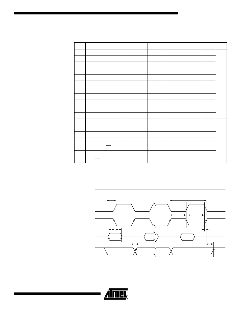
SPI Timing
Characteristics
See Figure 116 and Figure 117 for details.
Note:
1. In SPI Programming mode, the minimum SCK high/low period is:
– 2 t
CLCL
for f
CK
< 12 MHz
– 3 t
CLCL
for f
CK
> 12 MHz.
Figure 116. SPI Interface Timing Requirements (Master Mode)
Table 114. SPI Timing Parameters
Description
Mode
Min
Typ
Max
1
SCK period
Master
See Table 68
ns
2
SCK high/low
Master
50% duty cycle
3
Rise/Fall time
Master
3.6
4
Setup
Master
10
5
Hold
Master
10
6
Out to SCK
Master
0.5 • t
sck
7
SCK to out
Master
10
8
SCK to out high
Master
10
9
SS low to out
Slave
15
10
SCK period
Slave
4 • t
ck
11
SCK high/low
Slave
2 • t
ck
12
Rise/Fall time
Slave
1.6
µs
13
Setup
Slave
10
ns
14
Hold
Slave
t
ck
15
SCK to out
Slave
15
16
SCK to SS high
Slave
20
17
SS high to tri-state
Slave
10
18
SS low to SCK
Slave
2 • t
ck
MOSI
(Data Output)
SCK
(CPOL = 1)
MISO
(Data Input)
SCK
(CPOL = 0)
SS
MSB
LSB
LSB
MSB
...
...
6
1
2
2
3
4
5
8
7
- MAX5151 (16 pages)
- MAXQ3108 (64 pages)
- MAX5661 (39 pages)
- MAX6691 (7 pages)
- MAX5362 (12 pages)
- ADC10158 (26 pages)
- MAX8922L (14 pages)
- MAX8596Z (8 pages)
- MAX7491 (18 pages)
- MAX15040 (15 pages)
- MAX5177 (16 pages)
- ADC08138 (22 pages)
- MAX5961 (42 pages)
- T89C51RD2 (86 pages)
- MAX16055 (9 pages)
- MAX6659 (17 pages)
- ADC0820 (20 pages)
- MAX6678 (19 pages)
- MAX8884Z (15 pages)
- MAX16915 (9 pages)
- MAX8620 (18 pages)
- MAX5144 (12 pages)
- MAX6670 (8 pages)
- MAX8760 (39 pages)
- W78C32C (14 pages)
- MX7533 (8 pages)
- MAX8727 (13 pages)
- MAX9053 (15 pages)
- W78C54 (16 pages)
- MAX8614B (15 pages)
- W90N740 (219 pages)
- MAX6626 (13 pages)
- ADC10738 (30 pages)
- MAX17000 (31 pages)
- MAX5051 (21 pages)
- MAXQ1004 (18 pages)
- MAX6871 (51 pages)
- MX7847 (12 pages)
- MAX6608 (6 pages)
- MAX17083 (15 pages)
- MAX6641 (17 pages)
- MAX5251 (16 pages)
- MAX6338 (8 pages)
- MAX6690 (16 pages)
- MAX8668 (18 pages)