Table 102, Table 104, Atmega162/v – Rainbow Electronics ATmega162V User Manual
Page 234
234
ATmega162/V
2513E–AVR–09/03
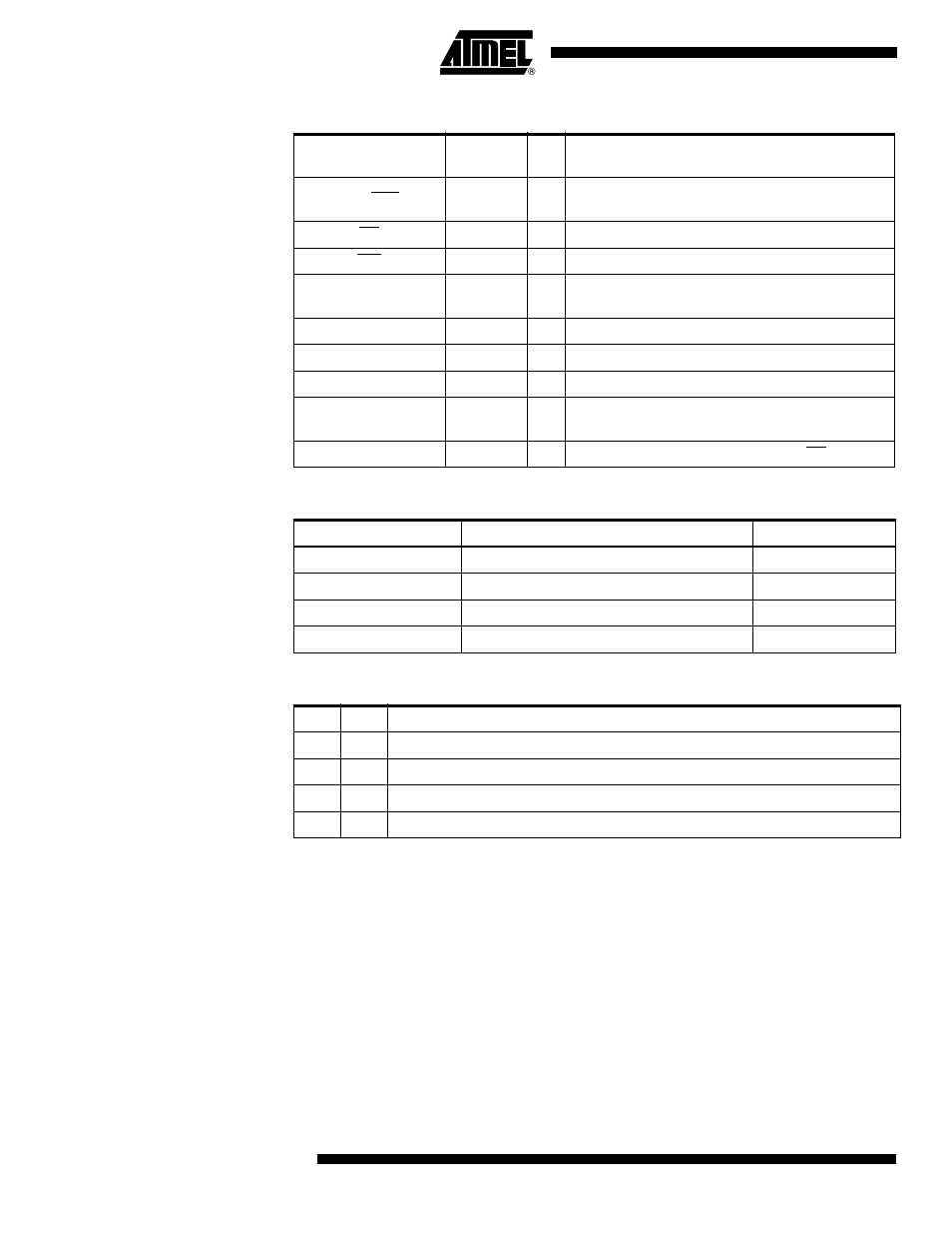
Table 102. Pin Name Mapping
Signal Name in
Programming Mode
Pin Name
I/O
Function
RDY/BSY
PD1
O
0: Device is busy programming, 1: Device is ready
for new command
OE
PD2
I
Output Enable (Active low)
WR
PD3
I
Write Pulse (Active low)
BS1
PD4
I
Byte Select 1 (“0” selects low byte, “1” selects high
byte)
XA0
PD5
I
XTAL Action Bit 0
XA1
PD6
I
XTAL Action Bit 1
PAGEL
PD7
I
Program Memory and EEPROM data Page Load
BS2
PA0
I
Byte Select 2 (“0” selects low byte, “1” selects 2’nd
high byte)
DATA
PB7 - 0
I/O
Bi-directional Data bus (Output when OE is low)
Table 103. Pin Values used to Enter Programming Mode
Pin
Symbol
Value
PAGEL
Prog_enable[3]
0
XA1
Prog_enable[2]
0
XA0
Prog_enable[1]
0
BS1
Prog_enable[0]
0
Table 104. XA1 and XA0 Coding
XA1
XA0
Action when XTAL1 is Pulsed
0
0
Load Flash or EEPROM address (High or low address byte determined by BS1)
0
1
Load Data (High or Low data byte for Flash determined by BS1).
1
0
Load Command
1
1
No Action, Idle
- MAX5151 (16 pages)
- MAXQ3108 (64 pages)
- MAX5661 (39 pages)
- MAX6691 (7 pages)
- MAX5362 (12 pages)
- ADC10158 (26 pages)
- MAX8922L (14 pages)
- MAX8596Z (8 pages)
- MAX7491 (18 pages)
- MAX15040 (15 pages)
- MAX5177 (16 pages)
- ADC08138 (22 pages)
- MAX5961 (42 pages)
- T89C51RD2 (86 pages)
- MAX16055 (9 pages)
- MAX6659 (17 pages)
- ADC0820 (20 pages)
- MAX6678 (19 pages)
- MAX8884Z (15 pages)
- MAX16915 (9 pages)
- MAX8620 (18 pages)
- MAX5144 (12 pages)
- MAX6670 (8 pages)
- MAX8760 (39 pages)
- W78C32C (14 pages)
- MX7533 (8 pages)
- MAX8727 (13 pages)
- MAX9053 (15 pages)
- W78C54 (16 pages)
- MAX8614B (15 pages)
- W90N740 (219 pages)
- MAX6626 (13 pages)
- ADC10738 (30 pages)
- MAX17000 (31 pages)
- MAX5051 (21 pages)
- MAXQ1004 (18 pages)
- MAX6871 (51 pages)
- MX7847 (12 pages)
- MAX6608 (6 pages)
- MAX17083 (15 pages)
- MAX6641 (17 pages)
- MAX5251 (16 pages)
- MAX6338 (8 pages)
- MAX6690 (16 pages)
- MAX8668 (18 pages)