Data polling flash, Data polling eeprom, See figure 106 – Rainbow Electronics ATmega162V User Manual
Page 246: Ee table 110, Table 110, Atmega162/v
246
ATmega162/V
2513E–AVR–09/03
6.
Any memory location can be verified by using the Read instruction which returns
the content at the selected address at serial output MISO.
7.
At the end of the programming session, RESET can be set high to commence
normal operation.
8.
Power-off sequence (if needed):
Set RESET to “1”.
Turn V
CC
power off.
Data Polling Flash
When a page is being programmed into the Flash, reading an address location within
the page being programmed will give the value 0xFF. At the time the device is ready for
a new page, the programmed value will read correctly. This is used to determine when
the next page can be written. Note that the entire page is written simultaneously and any
address within the page can be used for polling. Data polling of the Flash will not work
for the value 0xFF, so when programming this value, the user will have to wait for at
least t
WD_FLASH
before programming the next page. As a chip erased device contains
0xFF in all locations, programming of addresses that are meant to contain 0xFF, can be
skipped. See Table 110 for t
WD_FLASH
value.
Data Polling EEPROM
When a new byte has been written and is being programmed into EEPROM, reading the
address location being programmed will give the value 0xFF. At the time the device is
ready for a new byte, the programmed value will read correctly. This is used to deter-
mine when the next byte can be written. This will not work for the value 0xFF, but the
user should have the following in mind: As a chip erased device contains 0xFF in all
locations, programming of addresses that are meant to contain 0xFF, can be skipped.
This does not apply if the EEPROM is re-programmed without chip erasing the device.
In this case, data polling cannot be used for the value 0xFF, and the user will have to
wait at least t
W D _E E P ROM
before programming the next byte. See Table 110 for
t
WD_EEPROM
value.
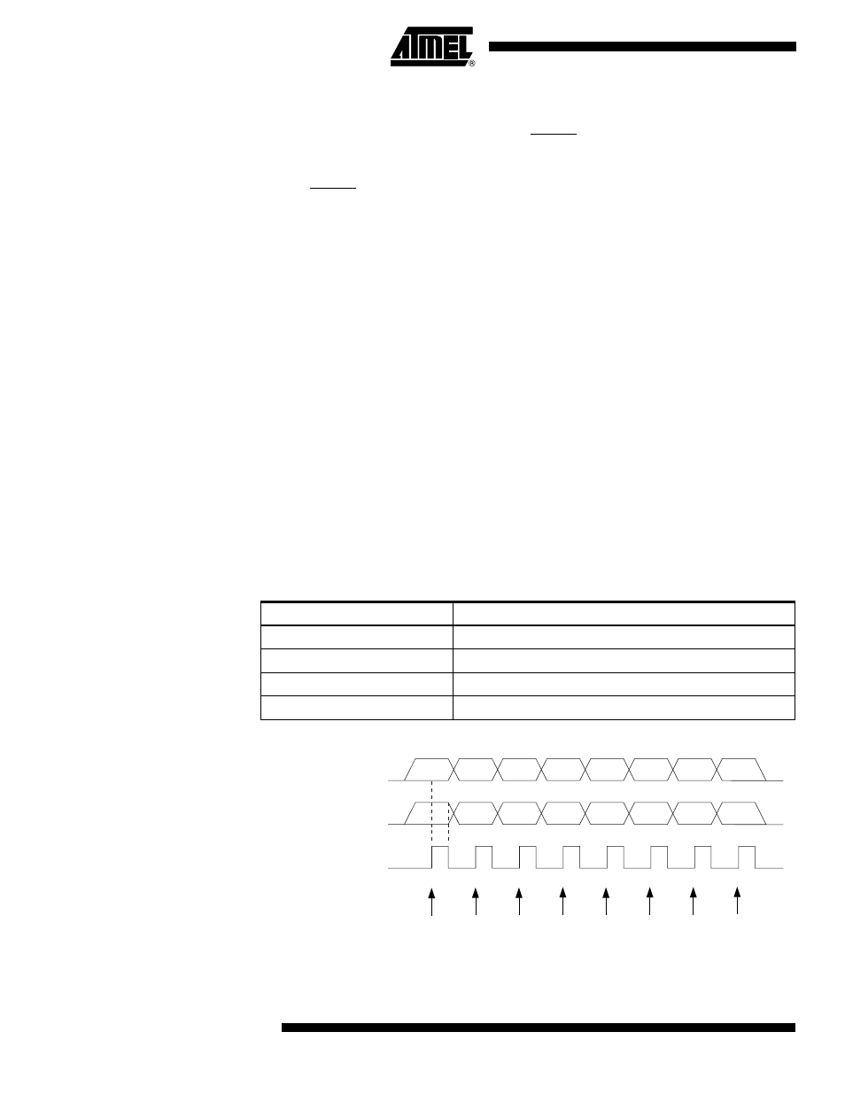
Figure 106. SPI Serial Programming Waveforms
Table 110. Minimum Wait Delay before Writing the Next Flash or EEPROM Location
Symbol
Minimum Wait Delay
t
WD_FLASH
4.5 ms
t
WD_EEPROM
9.0 ms
t
WD_ERASE
9.0 ms
t
WD_FUSE
4.5 ms
MSB
MSB
LSB
LSB
SERIAL CLOCK INPUT
(SCK)
SERIAL DATA INPUT
(MOSI)
(MISO)
SAMPLE
SERIAL DATA OUTPUT