Alternate functions of port b, Atmega162/v – Rainbow Electronics ATmega162V User Manual
Page 71
71
ATmega162/V
2513E–AVR–09/03
Alternate Functions Of Port B
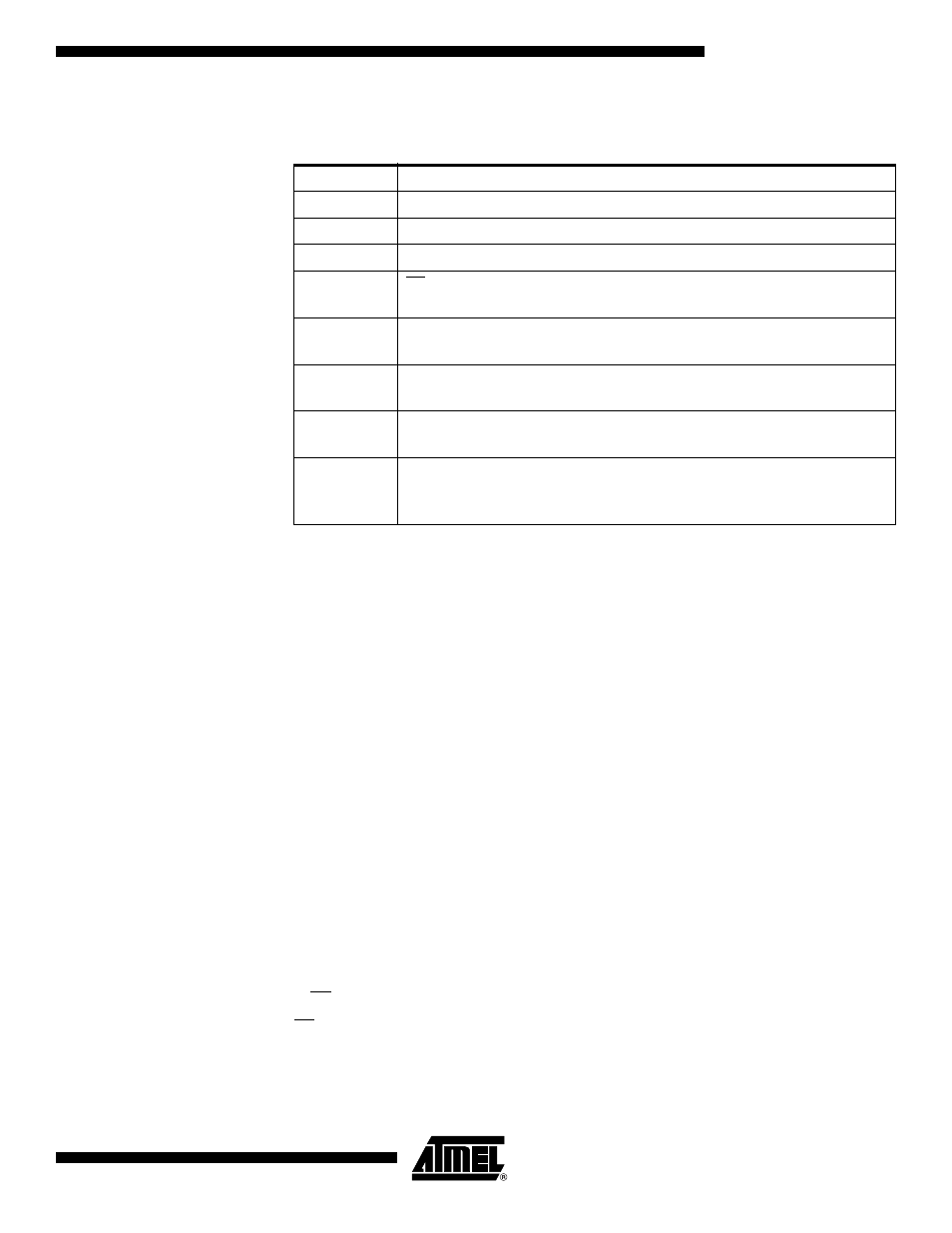
The Port B pins with alternate functions are shown in Table 32.
The alternate pin configuration is as follows:
• SCK – Port B, Bit 7
SCK: Master Clock output, Slave Clock input pin for SPI channel. When the SPI is
enabled as a Slave, this pin is configured as an input regardless of the setting of DDB7.
When the SPI is enabled as a Master, the data direction of this pin is controlled by
DDB7. When the pin is forced by the SPI to be an input, the pull-up can still be con-
trolled by the PORTB7 bit.
• MISO – Port B, Bit 6
MISO: Master Data input, Slave Data output pin for SPI channel. When the SPI is
enabled as a Master, this pin is configured as an input regardless of the setting of
DDB6. When the SPI is enabled as a Slave, the data direction of this pin is controlled by
DDB6. When the pin is forced by the SPI to be an input, the pull-up can still be con-
trolled by the PORTB6 bit.
• MOSI – Port B, Bit 5
MOSI: SPI Master Data output, Slave Data input for SPI channel. When the SPI is
enabled as a Slave, this pin is configured as an input regardless of the setting of DDB5.
When the SPI is enabled as a Master, the data direction of this pin is controlled by
DDB5. When the pin is forced by the SPI to be an input, the pull-up can still be con-
trolled by the PORTB5 bit.
• SS/OC3B – Port B, Bit 4
SS: Slave Select input. When the SPI is enabled as a slave, this pin is configured as an
input regardless of the setting of DDB4. As a Slave, the SPI is activated when this pin is
driven low. When the SPI is enabled as a Master, the data direction of this pin is con-
trolled by DDB4. When the pin is forced by the SPI to be an input, the pull-up can still be
controlled by the PORTB4 bit.
Table 32. Port B Pins Alternate Functions
Port Pin
Alternate Functions
PB7
SCK (SPI Bus Serial Clock)
PB6
MISO (SPI Bus Master Input/Slave Output)
PB5
MOSI (SPI Bus Master Output/Slave Input)
PB4
SS (SPI Slave Select Input)
OC3B (Timer/Counter3 Output Compare Match Output)
PB3
AIN1 (Analog Comparator Negative Input)
TXD1 (USART1 Output Pin)
PB2
AIN0 (Analog Comparator Positive Input)
RXD1 (USART1 Input Pin)
PB1
T1 (Timer/Counter1 External Counter Input)
OC2 (Timer/Counter2 Output Compare Match Output)
PB0
T0 (Timer/Counter0 External Counter Input)
OC0 (Timer/Counter0 Output Compare Match Output)
clk
I/O
(Divided System Clock)