Xmem register description, Mcu control register – mcucr, Extended mcu control register – emcucr – Rainbow Electronics ATmega162V User Manual
Page 28: Atmega162/v

28
ATmega162/V
2513E–AVR–09/03
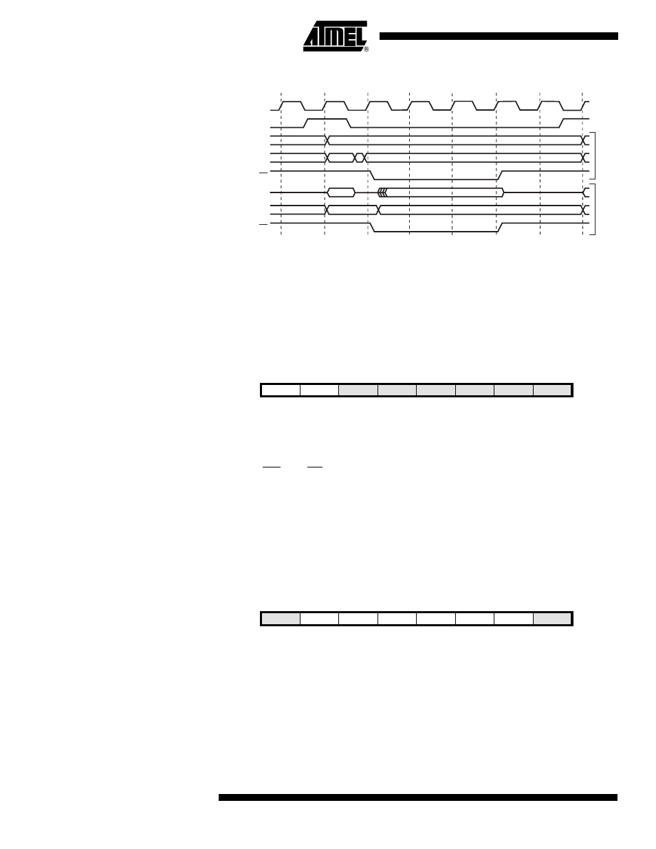
Figure 16. External Data Memory Cycles with SRWn1 = 1 and SRWn0 = 1
Note:
1. SRWn1 = SRW11 (upper sector) or SRW01 (lower sector), SRWn0 = SRW10 (upper
sector) or SRW00 (lower sector).
The ALE pulse in period T7 is only present if the next instruction accesses the RAM
(internal or external).
XMEM Register
Description
MCU Control Register –
MCUCR
• Bit 7 – SRE: External SRAM/XMEM Enable
Writing SRE to one enables the External Memory Interface.The pin functions AD7:0,
A15:8, ALE, WR, and RD are activated as the alternate pin functions. The SRE bit over-
rides any pin direction settings in the respective Data Direction Registers. Writing SRE
to zero, disables the External Memory Interface and the normal pin and data direction
settings are used.
• Bit 6 – SRW10: Wait State Select Bit
For a detailed description, see common description for the SRWn bits below (EMCUCR
description).
Extended MCU Control
Register – EMCUCR
• Bit 6..4 – SRL2, SRL1, SRL0: Wait State Sector Limit
It is possible to configure different wait-states for different external memory addresses.
The external memory address space can be divided in two sectors that have separate
wait-state bits. The SRL2, SRL1, and SRL0 bits select the splitting of these sectors, see
Table 2 and Figure 11. By default, the SRL2, SRL1, and SRL0 bits are set to zero and
the entire external memory address space is treated as one sector. When the entire
ALE
T1
T2
T3
Wr
ite
Read
WR
T7
A15:8
Address
Prev. addr.
DA7:0
Address
Data
Prev. data
XX
RD
DA7:0 (XMBK = 0)
Data
Address
Data
Prev. data
Address
DA7:0 (XMBK = 1)
System Clock (CLK
CPU
)
T4
T5
T6
Bit
7
6
5
4
3
2
1
0
SRE
SRW10
SE
SM1
ISC11
ISC10
ISC01
ISC00
MCUCR
Read/Write
R/W
R/W
R/W
R/W
R/W
R/W
R/W
R/W
Initial Value
0
0
0
0
0
0
0
0
Bit
7
6
5
4
3
2
1
0
SM0
SRL2
SRL1
SRL0
SRW01
SRW00
SRW11
ISC2
EMCUCR
Read/Write
R/W
R/W
R/W
R/W
R/W
R/W
R/W
R/W
Initial Value
0
0
0
0
0
0
0
0
