Memory programming, Program and data memory lock bits, Fuse bits – Rainbow Electronics ATmega103L User Manual
Page 92
ATmega603/103
92
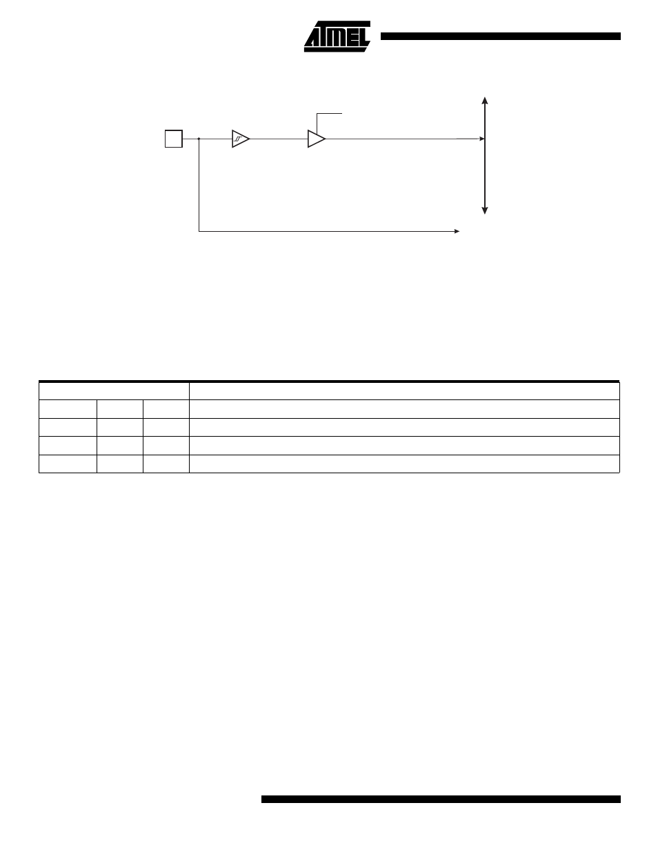
Figure 71. Port F Schematic Diagram (Pins PF7 - PF0)
Memory Programming
Program and Data Memory Lock Bits
The ATmega603/103 MCU provides two Lock bits which can be left unprogrammed (‘1’) or can be programmed (‘0’) to
obtain the additional features listed in Table 36. The Lock bits can only be erased to ‘1’ with the Chip Erase command..
Note:
1. In Parallel mode, programming of the Fuse bits are also disabled. Program the Fuse bits before programming the Lock bits.
Fuse Bits
The ATmega603/103 has four Fuse bits, SPIEN, SUT1..0, and EESAVE.
• When the SPIEN Fuse is programmed (‘0’), Serial Program and Data Downloading is enabled. Default value is
programmed (‘0’). The SPIEN Fuse is not accessible in serial programming mode.
• When EESAVE is programmed, the EEPROM memory is preserved through the Chip Erase cycle. Default value is
unprogrammed (‘1’). The EESAVE Fuse bit can not be programmed if any of the Lock bits are programmed.
• SUT1..0 Fuses: Determine the MCU start-up time. See Table 6 on page 26 for further details. Default value is un-
programmed (‘11’), which gives a nominal start up time of 16 ms.
The status of the Fuse bits is not affected by Chip Erase.
Table 36. Lock Bit Protection Modes
Memory Lock Bits
Protection Type
Mode
LB1
LB2
1
1
1
No memory lock features enabled.
2
0
1
Further programming of the Flash and EEPROM is disabled.
3
0
0
Same as mode 2, and verify is also disabled.
DA
T
A
B
US
PFn
AINn
TO ADC MUX
RP:
n:
READ PORTF PIN
0 - 7
RP