Port d data direction register - ddrd, Port d input pins address - pind, Port d as general digital i/o – Rainbow Electronics ATmega103L User Manual
Page 84: Alternate functions of port d, Int0 .. int3 - port d, bits 0, Ic1 - port d, bit 4, T1 - port d, bit 6, T2 - port d, bit 7
ATmega603/103
84
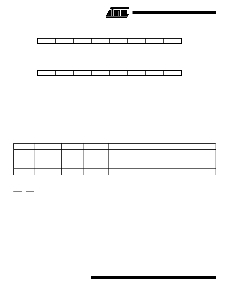
Port D Data Direction Register - DDRD
Port D Input Pins Address - PIND
The Port D Input Pins address - PIND - is not a register, and this address enables access to the physical value on each
Port D pin. When reading PORTD, the Port D Data Latch is read, and when reading PIND, the logical values present on the
pins are read.
Port D as general digital I/O
PDn, General I/O pin: The DDDn bit in the DDRD register selects the direction of this pin. If DDDn is set (one), PDn is con-
figured as an output pin. If DDDn is cleared (zero), PDn is configured as an input pin. If PDn is set (one) when configured
as an input pin the MOS pull up resistor is activated. To switch the pull up resistor off the PDn has to be cleared (zero) or
the pin has to be configured as an output pin.The port pins are tri-stated when a reset condition becomes active, even if the
clock is not running.
Note:
n: 7,6...0, pin number
Alternate Functions of Port D
INT0 .. INT3 - Port D, Bits 0..3
External Interrupt sources 0 - 3. The PD0 - PD3 pins can serve as external active low interrupt sources to the MCU. The
internal pull up MOS resistors can be activated as described above. See the interrupt description for further details, and
how to enable the sources.
IC1 - Port D, Bit 4
IC1 - Input Capture pin for Timer/Counter1. When a positive or negative (selectable) edge is applied to this pin, the con-
tents of Timer/Counter1 is transferred to the Timer/Counter1 Input Capture Register. The pin has to be configured as an
input to serve this function. See the Timer/Counter1 description on how to operate this function. The internal pull up MOS
resistor can be activated as described above.
T1 - Port D, Bit 6
T1, Timer/Counter1 counter source. See the timer description for further details.
T2 - Port D, Bit 7
T2, Timer/Counter2 counter source. See the timer description for further details.
Bit
7
6
5
4
3
2
1
0
$11
DDD7
DDD6
DDD5
DDD4
DDD3
DDD2
DDD1
DDD0
DDRD
Read/Write
R/W
R/W
R/W
R/W
R/W
R/W
R/W
R/W
Initial value
0
0
0
0
0
0
0
0
Bit
7
6
5
4
3
2
1
0
$10
PIND7
PIND6
PIND5
PIND4
PIND3
PIND2
PIND1
PIND0
PIND
Read/Write
R
R
R
R
R
R
R
R
Initial value
Hi-Z
Hi-Z
Hi-Z
Hi-Z
Hi-Z
Hi-Z
Hi-Z
Hi-Z
Table 33. DDDn Bits on Port D Pins
DDDn
PORTDn
I/O
Pull up
Comment
0
0
Input
No
Tri-state (Hi-Z)
0
1
Input
Yes
PDn will source current if ext. pulled low.
1
0
Output
No
Push-Pull Zero Output
1
1
Output
No
Push-Pull One Output