Rainbow Electronics ATmega103L User Manual
Page 18
ATmega603/103
18
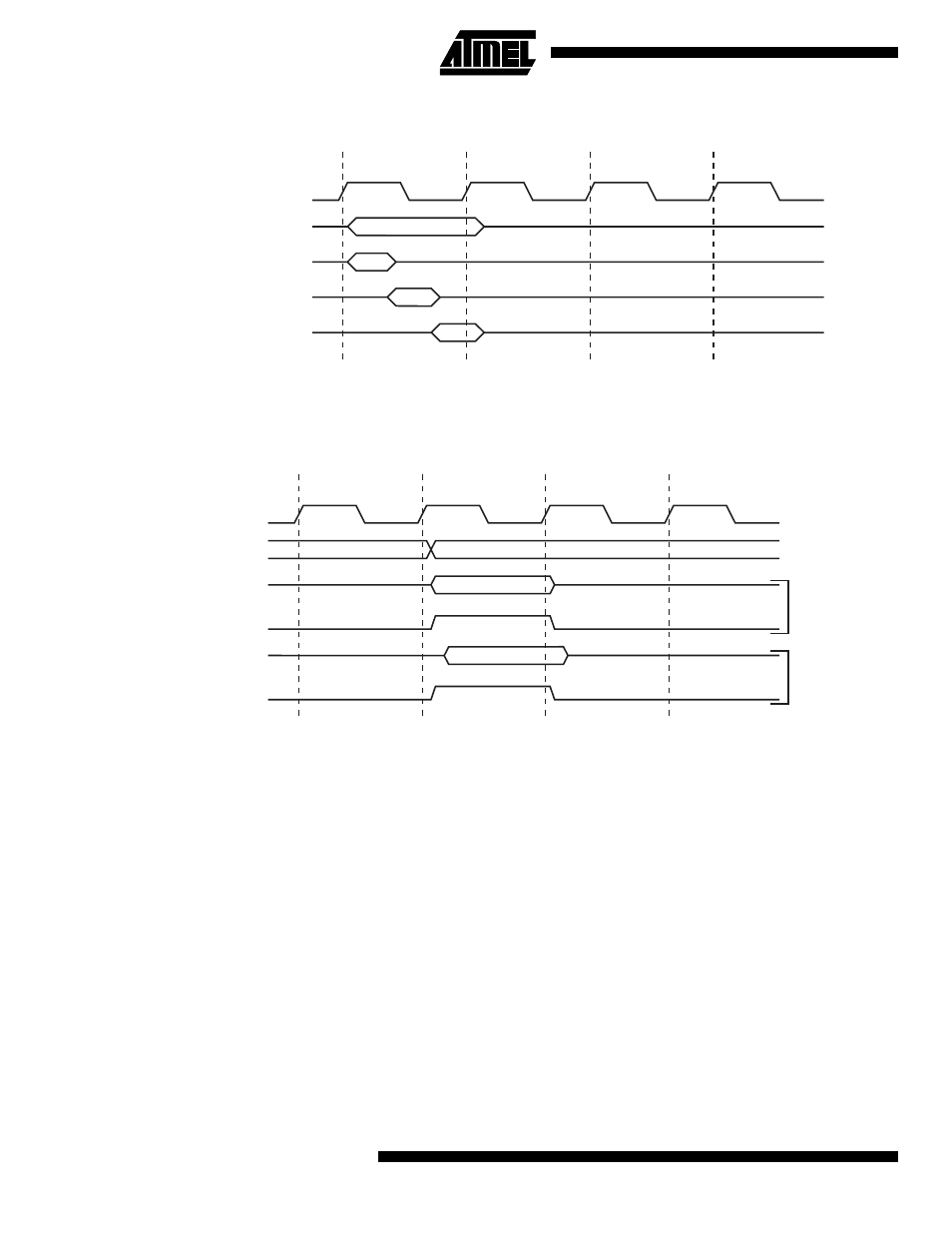
Figure 21. Single Cycle ALU Operation
The internal data SRAM access is performed in two System Clock cycles as described in Figure 22.
Figure 22. On-Chip Data SRAM Access Cycles
See “Interface to external SRAM” on page 72 for a description of the access to the external SRAM.
System Clock Ø
Total Execution Time
Register Operands Fetch
ALU Operation Execute
Result Write Back
T1
T2
T3
T4
System Clock Ø
WR
RD
Data
Data
Address
Address
T1
T2
T3
T4
Prev. Address
Read
Wr
ite
See also other documents in the category Rainbow Electronics Sensors:
- MAX5151 (16 pages)
- MAXQ3108 (64 pages)
- MAX5661 (39 pages)
- MAX6691 (7 pages)
- MAX5362 (12 pages)
- ADC10158 (26 pages)
- MAX8922L (14 pages)
- MAX8596Z (8 pages)
- MAX7491 (18 pages)
- MAX15040 (15 pages)
- MAX5177 (16 pages)
- ADC08138 (22 pages)
- MAX5961 (42 pages)
- T89C51RD2 (86 pages)
- MAX16055 (9 pages)
- MAX6659 (17 pages)
- ADC0820 (20 pages)
- MAX6678 (19 pages)
- MAX8884Z (15 pages)
- MAX16915 (9 pages)
- MAX8620 (18 pages)
- MAX5144 (12 pages)
- MAX6670 (8 pages)
- MAX8760 (39 pages)
- W78C32C (14 pages)
- MX7533 (8 pages)
- MAX8727 (13 pages)
- MAX9053 (15 pages)
- W78C54 (16 pages)
- MAX8614B (15 pages)
- W90N740 (219 pages)
- MAX6626 (13 pages)
- ADC10738 (30 pages)
- MAX17000 (31 pages)
- MAX5051 (21 pages)
- MAXQ1004 (18 pages)
- MAX6871 (51 pages)
- MX7847 (12 pages)
- MAX6608 (6 pages)
- MAX17083 (15 pages)
- MAX6641 (17 pages)
- MAX5251 (16 pages)
- MAX6338 (8 pages)
- MAX6690 (16 pages)
- MAX8668 (18 pages)