Asynchronous status register - assr – Rainbow Electronics ATmega103L User Manual
Page 41
ATmega603/103
41
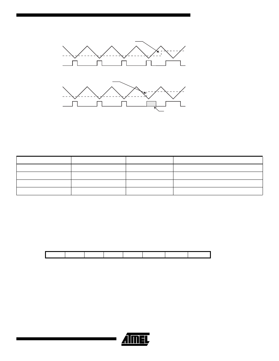
Figure 32. Effects on Unsynchronized OCR Latching
During the time between the write and the latch operation, a read from OCR0 or OCR2 will read the contents of the tempo-
rary location. This means that the most recently written value always will read out of OCR0/2
When the OCR register (not the temporary register) is updated to $00 or $FF, the PWM output changes to low or high
immediately according to the settings of COM21/COM20 or COM11/COM10. This is shown in Table 15:
Note:
n = 0 or 2
In PWM mode, the Timer Overflow Flag, TOV0 or TOV2, is set when the counter advances from $00. Timer Overflow
Interrupt0 and 2 operates exactly as in normal Timer/Counter mode, i.e. it is executed when TOV0 or TOV2 is set provided
that Timer Overflow Interrupt and global interrupts are enabled. This does also apply to the Timer Output Compare flags
and interrupts.
The frequency of the PWM will be Timer Clock Frequency divided by 510.
Asynchronous Status Register - ASSR
•
Bit 7..4 - Res: Reserved Bits
These bits are reserved bits in the ATmega603/103 and always reads as zero.
•
Bit 3 - AS0: Asynchronous Timer/Counter0
When set(one) Timer/Counter0 is clocked from the TOSC1 pin. When cleared (zero) Timer/Counter0 is clocked from the
internal system clock, CK. When the value of this bit is changed the contents of TCNT0 might get corrupted.
•
Bit 2 - TCN0UB: Timer/Counter0 Update Busy
When Timer/Counter0 operates asynchronously and TCNT0 is written, this bit becomes set (one). When TCNT0 has been
updated from the temporary storage register, this bit is cleared (zero) by hardware. A logical zero in this bit indicates that
TCNT0 is ready to be updated with a new value.
Table 15. PWM Outputs OCRn = $00 or $FF
COMn1
COMn0
OCRn
Output PWMn
1
0
$00
L
1
0
$FF
H
1
1
$00
H
1
1
$FF
L
Bit
7
6
5
4
3
2
1
0
$30 ($50)
-
-
-
-
AS0
TCN0UB
OCR0UB
TCR0UB
ASSR
Read/Write
R
R
R
R
R/W
R
R
R
Initial value
0
0
0
0
0
0
0
0
Counter Value
Compare Value
PWM Output
Synchronized OCR Latch
Counter Value
Compare Value
PWM Output
Unsynchronized OCR Latch
Glitch
Compare Value changes
Compare Value changes