Relative program addressing, rjmp and rcall, Eeprom data memory – Rainbow Electronics ATmega103L User Manual
Page 17
ATmega603/103
17
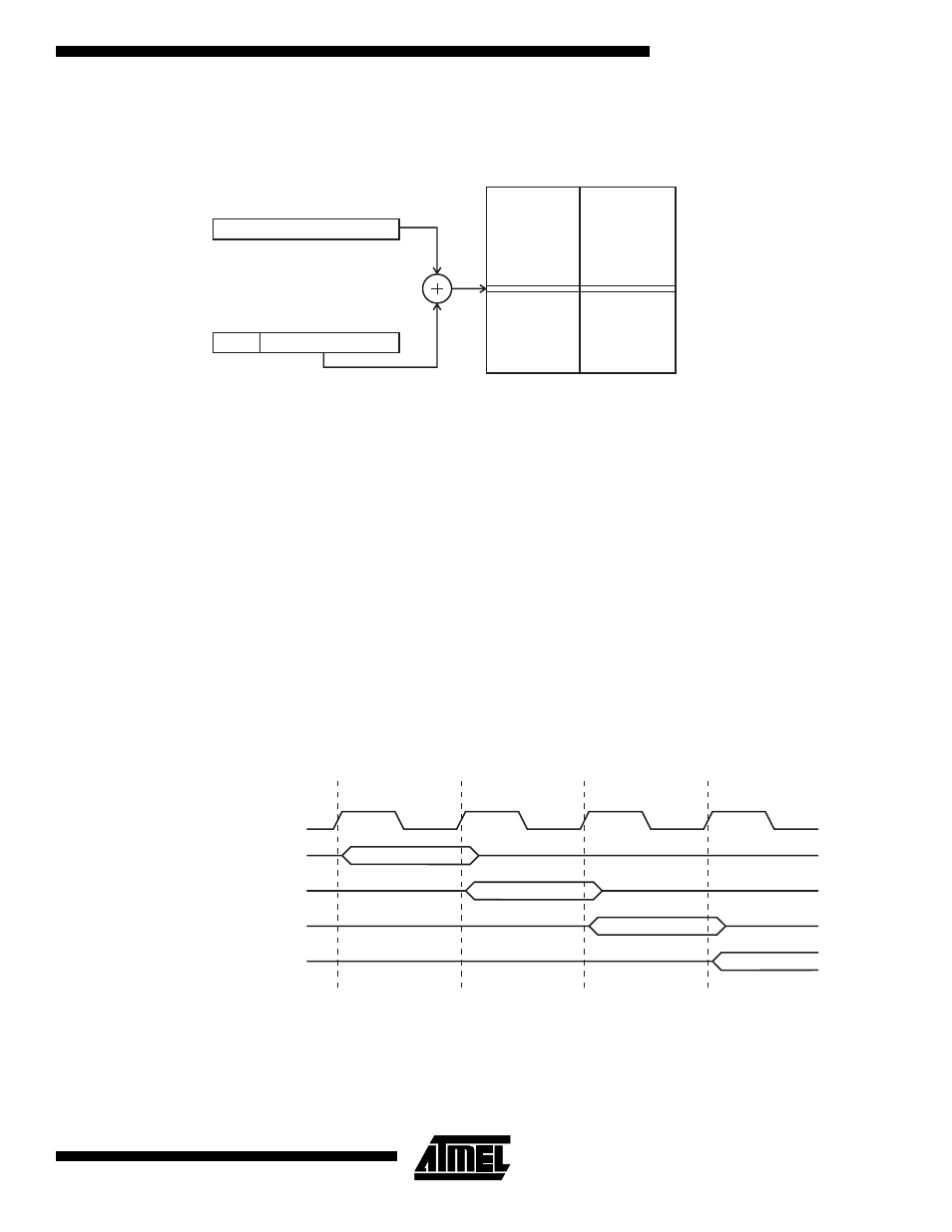
Relative Program Addressing, RJMP and RCALL
Figure 19. Relative Program Memory Addressing
Program execution continues at address PC + k + 1. The relative address k is -2048 to 2047.
EEPROM Data Memory
The EEPROM memory is organized as a separate data space, in which single bytes can be read and written. The
EEPROM has an endurance of at least 100,000 write/erase cycles. The access between the EEPROM and the CPU is
described on page 52 specifying the EEPROM address register, the EEPROM data register, and the EEPROM control
register.
Memory Access Times and Instruction Execution Timing
This section describes the general access timing concepts for instruction execution and internal memory access.
The AVR CPU is driven by the System Clock Ø, directly generated from the external clock crystal for the chip. No internal
clock division is used.
Figure 20 shows the parallel instruction fetches and instruction executions enabled by the Harvard architecture and the
fast-access register file concept. This is the basic pipelining concept to obtain up to 1 MIPS per MHz with the corresponding
unique results for functions per cost, functions per clocks, and functions per power-unit.
Figure 20. The Parallel Instruction Fetches and Instruction Executions
Figure 21 shows the internal timing concept for the register file. In a single clock cycle an ALU operation using two register
operands is executed, and the result is stored back to the destination register.
PC
0
0
15
15
11
12
OP
k
PROGRAM MEMORY
$0000
$7FFF/$FFFF
System Clock Ø
1st Instruction Fetch
1st Instruction Execute
2nd Instruction Fetch
2nd Instruction Execute
3rd Instruction Fetch
3rd Instruction Execute
4th Instruction Fetch
T1
T2
T3
T4