Timer/counter0 output compare register - ocr0, Timer/counter2 output compare register - ocr2, Timer/counter 0 and 2 in pwm mode – Rainbow Electronics ATmega103L User Manual
Page 40
ATmega603/103
40
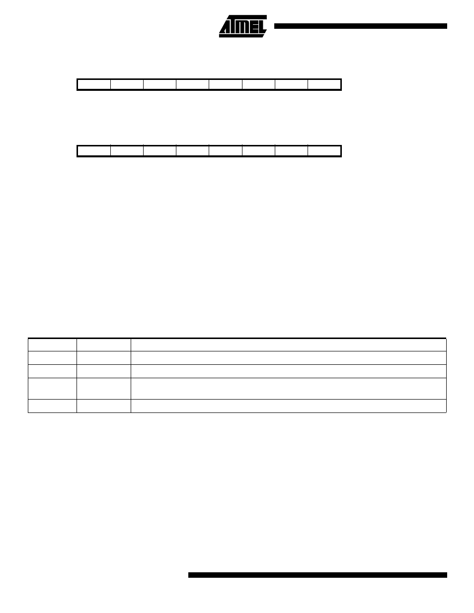
Timer/Counter0 Output Compare Register - OCR0
Timer/Counter2 Output Compare Register - OCR2
The output compare registers are 8-bit read/write registers.
The Timer/Counter Output Compare Registers contain the data to be continuously compared with the Timer/Counter.
Actions on compare matches are specified in TCCR0 and TCCR2. A compare match does only occur if the Timer/Counter
counts to the OCR value. A software write that sets the Timer/Counter and Output Compare Register to the same value
does not generate a compare match.
A compare match will set the compare interrupt flag in the CPU clock cycle following the compare event.
Timer/Counter 0 and 2 in PWM mode
When the PWM mode is selected, the Timer/Counter and the Output Compare Register - OCR0 or OCR2 form an 8-bit,
free-running, glitch-free and phase correct PWM with outputs on the PB4(OC0/PWM0) or PB7(OC2/PWM2) pin. The
Timer/Counter acts as an up/down counter, counting up from $00 to $FF, where it turns and counts down again to zero
before the cycle is repeated. When the counter value matches the contents of the Output Compare register, the
PB4(OC0/PWM0) or PB7(OC2/PWM2) pin is set or cleared according to the settings of the COM01/COM00 or
COM21/COM20 bits in the Timer/Counter Control Registers TCCR0 and TCCR2. Refer to Table 14 for details.
Note:
n = 0 or 2
Note that in PWM mode, the Output Compare register is transferred to a temporary location when written. The value is
latched when the Timer/Counter reaches $FF. This prevents the occurrence of odd-length PWM pulses (glitches) in the
event of an unsynchronized OCR0 or OCR2 write. See Figure 32 for an example.
Bit
7
6
5
4
3
2
1
0
$31 ($51)
MSB
LSB
OCR0
Read/Write
R/W
R/W
R/W
R/W
R/W
R/W
R/W
R/W
Initial value
0
0
0
0
0
0
0
0
Bit
7
6
5
4
3
2
1
0
$23 ($43)
MSB
LSB
OCR2
Read/Write
R/W
R/W
R/W
R/W
R/W
R/W
R/W
R/W
Initial value
0
0
0
0
0
0
0
0
Table 14. Compare Mode Select in PWM Mode
COMn1
COMn0
Effect on Compare/PWM Pin
0
0
Not connected
0
1
Not connected
1
0
Cleared on compare match, up-counting. Set on compare match, down-counting (non-inverted
PWM).
1
1
Cleared on compare match, down-counting. Set on compare match, up-counting (inverted PWM).