Adc data register - adcl and adch, Adc noise canceling techniques – Rainbow Electronics ATmega103L User Manual
Page 71
ATmega603/103
71
ADC Data Register - ADCL and ADCH
When an ADC conversion is complete, the result is found in these two registers. It is essential that both registers are read,
and that ADCL is read before ADCH.
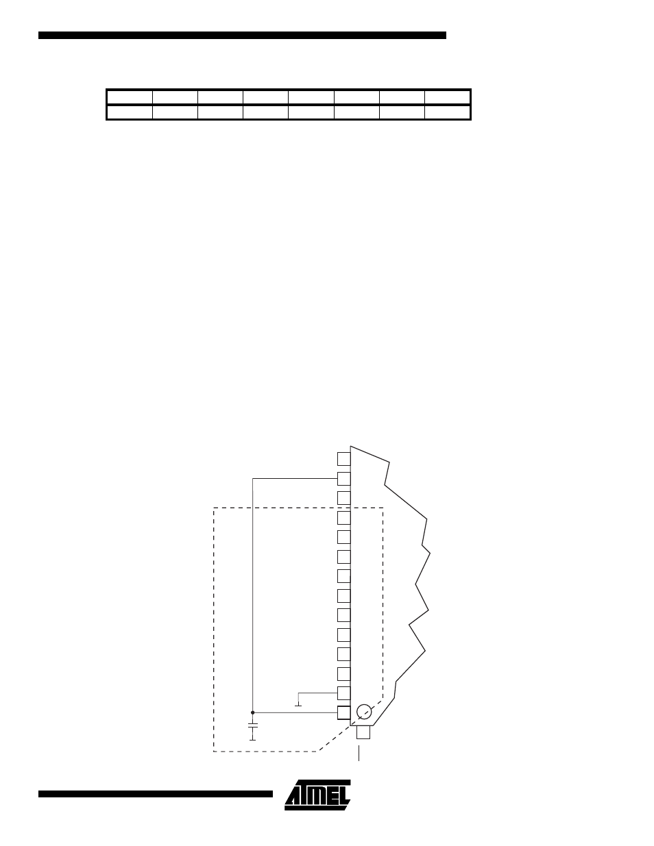
ADC Noise Canceling Techniques
Digital circuitry inside and outside the ATmega603/103 generates EMI which might affect the accuracy of analog measure-
ments. If conversion accuracy is critical, the noise level can be reduced by applying the following techniques:
1.
The analog part of the ATmega603/103 and all analog components in the application should have a separate ana-
log ground plane on the PCB. This ground plane is connected to the digital ground plane via a single point on the
PCB.
2.
Keep analog signal paths as short as possible. Make sure analog tracks run over the analog ground plane, and keep
them well away from high-speed switching digital tracks.
3.
The AV
CC
pin on the ATmega603/103 should have its own decoupling capacitor as shown in Figure 49.
4.
Use the ADC noise canceler function to reduce induced noise from the CPU.
5.
If some Port F pins are used as digital inputs, it is essential that these do not switch while a conversion is in
progress.
Figure 49. ADC Power Connections
Bit
15
14
13
12
11
10
9
8
$05 ($25)
-
-
-
-
-
-
ADC9
ADC8
ADCH
$04 ($24)
ADC7
ADC6
ADC5
ADC4
ADC3
ADC2
ADC1
ADC0
ADCL
7
6
5
4
3
2
1
0
Read/Write
R
R
R
R
R
R
R
R
R
R
R
R
R
R
R
R
Initial value
0
0
0
0
0
0
0
0
0
0
0
0
0
0
0
0
VCC
GND
10nF
Analog Ground Plane
A
Tmega603/103
(ADC0) PF0
(ADC7) PF7
(ADC1) PF1
(ADC2) PF2
(ADC3) PF3
(ADC4) PF4
(ADC5) PF5
(ADC6) PF6
AREF
AGND
AVCC
52
53
54
55
56
57
58
59
60
61
61
62
62
63
63
64
64
1
51
PEN
(AD0) PA0