Operation – Rainbow Electronics ATmega103L User Manual
Page 67
ATmega603/103
67
An external reference voltage must be applied to the AREF pin. This voltage must be in the range AGND - AV
CC
.
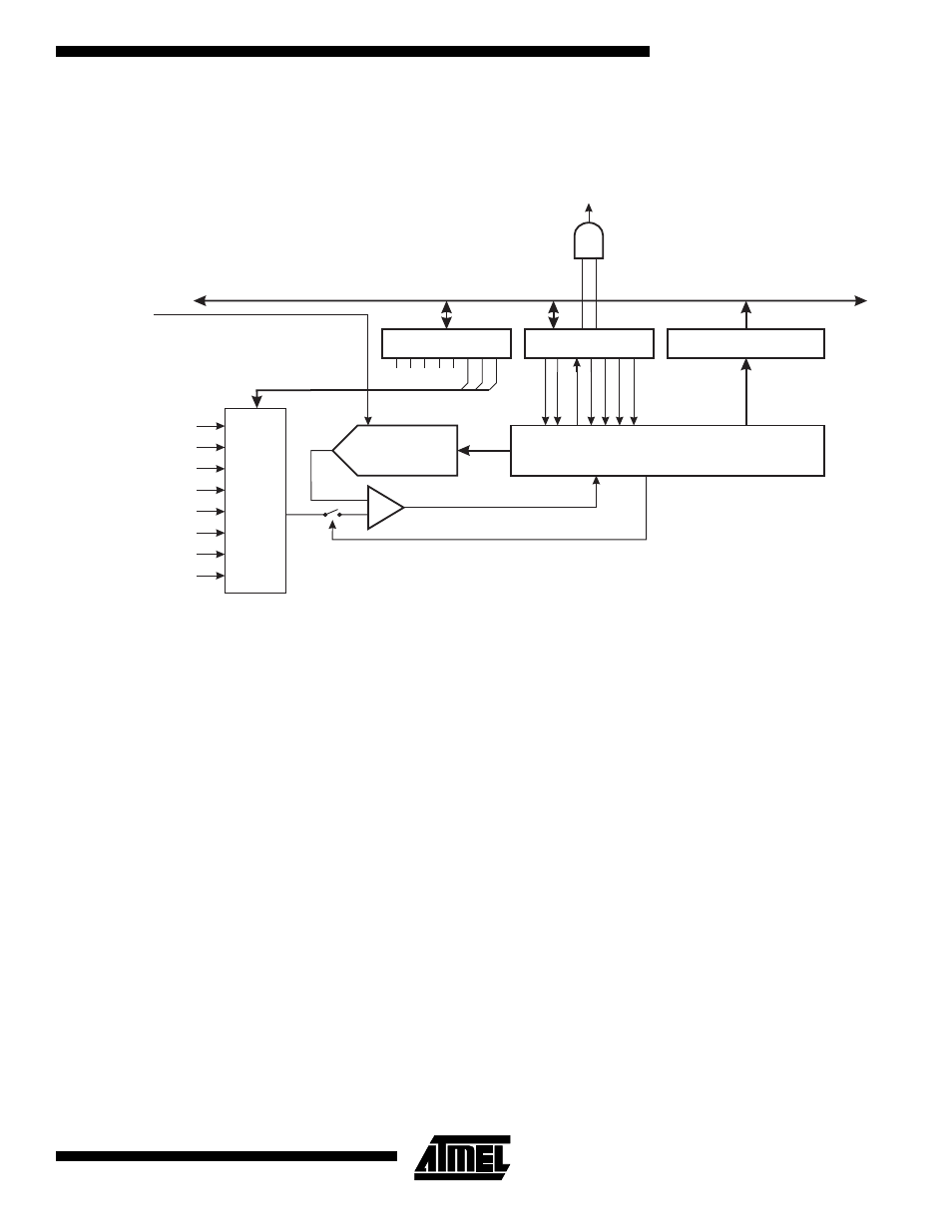
Figure 45. Analog to Digital Converter Block Schematic
Operation
The ADC operates in Single Conversion mode, and each conversion will have to be initiated by the user.
The ADC is enabled by writing a logical one to the ADC Enable bit, ADEN in ADCSR. The first conversion that is started
after enabling the ADC, will be preceded by a dummy conversion to initialize the ADC. To the user, the only difference will
be that this conversion takes 13 more ADC clock pulses than a normal conversion. (See Figure 48.)
A conversion is started by writing a logical one to the ADC Start Conversion bit, ADSC. This bit will stay high as long as the
conversion is in progress and be set to zero by hardware when the conversion is completed. If a different data channel is
selected while a conversion is in progress, the ADC will finish the current conversion before performing the channel
change.
As the ADC generates a 10-bit result, two data registers, ADCH and ADCL, must be read to get the result when the conver-
sion is complete. Special data protection logic is used to ensure that the contents of the data registers belong to the same
result when they are read. This mechanism works as follows:
When reading data, ADCL must be read first. Once ADCL is read, ADC access to data registers is blocked. This means
that if ADCL has been read, and a conversion completes before ADCH is read, none of the registers are updated and the
result from the conversion is lost. When ADCH is read, ADC access to the ADCH and ADCL registers is re-enabled.
The ADC has its own interrupt, ADIF, which can be triggered when a conversion completes. When ADC access to the data
registers is prohibited between reading of ADCL and ADCH, the interrupt will trigger even if the result is lost.
ADC CONVERSION
COMPLETE IRQ
8-BIT DATA BUS
9
0
ADC MULTIPLEXER
SELECT (ADMUX)
ADC CTRL & STATUS
REGISTER (ADCSR)
ADC DATA REGISTER
(ADCH/ADCL)
MUX2
ADIE
ADIE
ADSC
ADEN
ADIF
ADIF
MUX1
MUX0
ADPS0
ADPS1
ADPS2
8-
CHANNEL
MUX
CONVERSION LOGIC
10-BIT DAC
+
-
SAMPLE & HOLD
COMPARATOR
Analog
Inputs
External
Reference
Voltage