Rainbow Electronics ATmega103L User Manual
Page 44
ATmega603/103
44
Figure 33. Timer/Counter1 Block Diagram
Timer/Counter1 can also be used as a 8, 9 or 10-bit Pulse With Modulator. In this mode the counter and the
OCR1A/OCR1B registers serve as a dual glitch-free stand-alone PWM with centered pulses. Refer to page 49 for a
detailed description on this function.
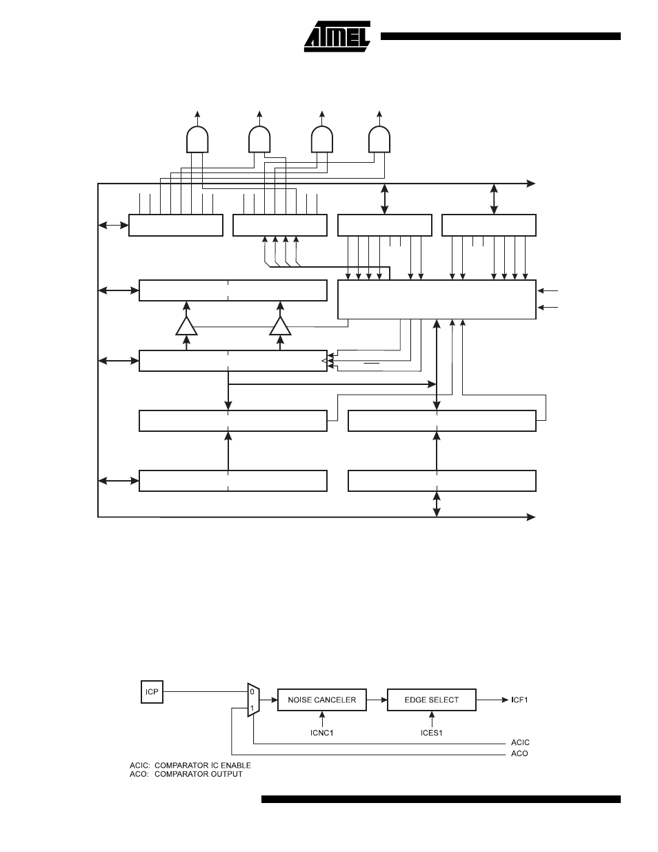
The Input Capture function of Timer/Counter1 provides a capture of the Timer/Counter1 contents to the Input Capture
Register - ICR1, triggered by an external event on the Input Capture Pin - PD4/(IC1). The actual capture event settings
are defined by the Timer/Counter1 Control Register - TCCR1B. In addition, the Analog Comparator can be set to trigger
the Input Capture. Refer to the paragraph, “The Analog Comparator”, for details on this. The ICP pin logic is shown
in Figure 34.
Figure 34. ICP Pin Schematic Diagram
8-BIT D
A
T
A
B
U
S
T/C1 CONTROL
REGISTER B (TCCR1B)
T/C1 CONTROL
REGISTER A (TCCR1A)
T/C1 INPUT CAPTURE REGISTER (ICR1)
16 BIT COMPARATOR
16 BIT COMPARATOR
TIMER/COUNTER1 OUTPUT COMPARE REGISTER A
TIMER/COUNTER1 OUTPUT COMPARE REGISTER B
TIMER/COUNTER1 (TCNT1)
TIMER INT. FLAG
REGISTER (TIFR)
0
0
0
0
0
0
7
7
7
7
7
7
8
8
8
8
8
8
15
15
15
15
15
15
CONTROL
LOGIC
COM1A1
COM1B1
CS12
TO
V
1
TO
V
1
OCF0
TO
V
0
OCF1A
OCF1A
OCF1B
OCF1B
ICF1
ICF1
COM1A0
COM1B0
CS1
1
CTC1
PWM1
1
PWM10
ICES1
ICNC1
CS10
CK
T/C1 COMPARE
MATCHA IRQ
T/C1 COMPARE
MATCHB IRQ
T/C1 INPUT
CAPTURE IRQ
T/C1 OVER-
FLOW IRQ
CAPTURE
TRIGGER
T/C CLOCK SOURCE
T/C CLEAR
UP/DOWN
TIMER INT. MASK
REGISTER (TIMSK)
OCIE0
T
OIE0
T
OIE1
OCIE1A
OCIE1B
TICIE1
T
OIE2
TO
V
2
OCIE2
OCF2
6