Data modes, Spi control register - spcr – Rainbow Electronics ATmega103L User Manual
Page 57
ATmega603/103
57
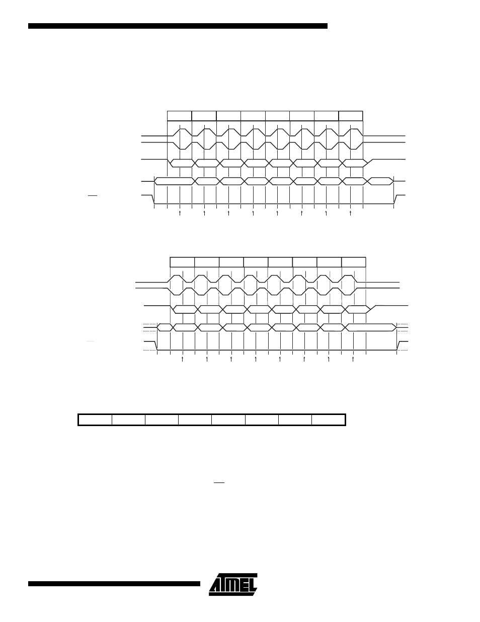
Data Modes
There are four combinations of SCK phase and polarity with respect to serial data, which are determined by control bits
CPHA and CPOL. The SPI data transfer formats are shown in Figure 39 and Figure 40.
Figure 39. SPI Transfer Format with CPHA = 0 and DORD = 0
Figure 40. SPI Transfer Format with CPHA = 1and DORD = 0
SPI Control Register - SPCR
•
Bit 7 - SPIE: SPI Interrupt Enable
This bit causes the SPI interrupt to be executed if SPIF bit in the SPSR register is set and the global interrupts are enabled.
•
Bit 6 - SPE: SPI Enable
When the SPE bit is set (one), the SPI is enabled and SS, MOSI, MISO and SCK are connected to pins PB0, PB1, PB2 and
PB3.
•
Bit 5 - DORD: Data Order
When the DORD bit is set (one), the LSB of the data word is transmitted first.
When the DORD bit is cleared (zero), the MSB of the data word is transmitted first.
Bit
7
6
5
4
3
2
1
0
$0D ($2D)
SPIE
SPE
DORD
MSTR
CPOL
CPHA
SPR1
SPR0
SPCR
Read/Write
R/W
R/W
R/W
R/W
R/W
R/W
R/W
R/W
Initial value
0
0
0
0
0
0
0
0
MSB
6
5
4
3
2
1
LSB
1
2
3
4
5
6
7
8
MSB
6
5
4
3
2
1
LSB
*
SCK CYCLE #
(FOR REFERENCE)
SCK (CPOL=0)
SCK (CPOL=1)
MOSI
(FROM MASTER)
MISO
(FROM SLAVE)
SS (TO SLAVE)
* Not defined but normally MSB of character just received
SAMPLE
1
1
1
2
2
2
3
3
3
4
4
4
5
5
5
6
6
6
*
7
8
SCK CYCLE #
(FOR REFERENCE)
SCK (CPOL=0)
SCK (CPOL=1)
MOSI
(FROM MASTER)
MISO
(FROM SLAVE)
SS (TO SLAVE)
* Not defined but normally LSB of previously transmitted character.
MSB
LSB
LSB
MSB
SAMPLE