Eeprom data register - eedr, Eeprom control register - eecr – Rainbow Electronics ATmega103L User Manual
Page 53
ATmega603/103
53
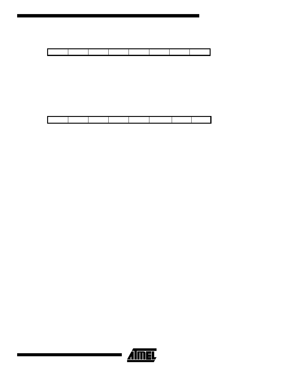
EEPROM Data Register - EEDR
•
Bits 7..0 - EEDR7..0: EEPROM Data:
For the EEPROM write operation, the EEDR register contains the data to be written to the EEPROM in the address given
by the EEAR register. For the EEPROM read operation, the EEDR contains the data read out from the EEPROM at the
address given by EEAR.
EEPROM Control Register - EECR
•
Bits 7..4 - Res: Reserved bits
These bits are reserved bits in the ATmega603/103 and will always be read as zero.
•
Bit 3 - EERIE: EEPROM Ready Interrupt Enable
When the I bit in SREG and EERIE are set (one), the EEPROM Ready Interrupt is enabled. When cleared (zero), the inter-
rupt is disabled. The EEPROM Ready interrupt constantly generates an interrupt request when EEWE is cleared (zero).
•
Bit 2 - EEMWE: EEPROM Master Write Enable
The EEMWE bit determines whether setting EEWE to one causes the EEPROM to be written. When EEMWE is set(one)
setting EEWE will write data to the EEPROM at the selected address If EEMWE is zero, setting EEWE will have no effect.
When EEMWE has been set (one) by software, hardware clears the bit to zero after four clock cycles. See the description
of the EEWE bit for a EEPROM write procedure.
•
Bit 1 - EEWE: EEPROM Write Enable
The EEPROM Write Enable Signal EEWE is the write strobe to the EEPROM. When address and data are correctly set up,
the EEWE bit must be set to write the value into the EEPROM. The EEMWE bit must be set when the logical one is written
to EEWE, otherwise no EEPROM write takes place. The following procedure should be followed when writing the
EEPROM (the order of steps 2 and 3 is unessential):
1.
Wait until EEWE becomes zero.
2.
Write new EEPROM address to EEAR (optional)
3.
Write new EEPROM data to EEDR (optional)
4.
Write a logical one to the EEMWE bit in EECR
5.
Within four clock cycles after setting EEMWE, write a logical one to EEWE.
Caution: An interrupt between step 4 and step 5 will make the write cycle fail, since the EEPROM Master Write Enable will
time-out. If an interrupt routine accessing the EEPROM is interrupting another EEPROM access, the EEAR and EEDR reg-
ister will be modified, causing the interrupted EEPROM access to fail. It is recommended to have the global interrupt flag
cleared during the 4 last steps to avoid these problems.
When the write access time (typically 2.5 ms at V
CC
= 5V or 4 ms at V
CC
= 2.7V) has elapsed, the EEWE bit is cleared
(zero) by hardware. The user software can poll this bit and wait for a zero before writing the next byte. When EEWE has
been set, the CPU is halted for two cycles before the next instruction is executed.
•
Bit 0 - EERE: EEPROM Read Enable
The EEPROM Read Enable Signal EERE is the read strobe to the EEPROM. When the correct address is set up in the
EEAR register, the EERE bit must be set. When the EERE bit is cleared (zero) by hardware, requested data is found in the
EEDR register. The EEPROM read access takes one instruction there is no need to poll the EERE bit. When EERE has
been set, the CPU is halted for four cycles before the next instruction is executed.
Bit
7
6
5
4
3
2
1
0
$1D ($3D)
MSB
LSB
EEDR
Read/Write
R/W
R/W
R/W
R/W
R/W
R/W
R/W
R/W
Initial value
0
0
0
0
0
0
0
0
Bit
7
6
5
4
3
2
1
0
$1C ($3C)
-
-
-
-
EERIE
EEMWE
EEWE
EERE
EECR
Read/Write
R
R
R
R
R
R/W
R/W
R/W
Initial value
0
0
0
0
0
0
0
0