Timer/counter0 control register - tccr0, Timer/counter2 control register - tccr2 – Rainbow Electronics ATmega103L User Manual
Page 38
ATmega603/103
38
Timer/Counter0 Control Register - TCCR0
Timer/Counter2 Control Register - TCCR2
•
Bit 7 - Res: Reserved Bit
This bit is a reserved bit in the ATmega603/103 and always reads as zero.
•
Bit 6 - PWM0 / PWM2: Pulse Width Modulator Enable
When set (one) this bit enables PWM mode for Timer/Counter0 or Timer/Counter2. This mode is described on page 40.
•
Bits 5,4 - COM01, COM00 / COM21, COM20: Compare Output Mode, bits 1 and 0
The COMn1 and COMn0 control bits determine any output pin action following a compare match in Timer/Counter2.
Any output pin actions affect pins PB4(OC0/PWM0) or PB7(OC2/PWM2). Since this is an alternative function to an I/O
port, the corresponding direction control bit must be set (one) to control an output pin. The control configuration is shown in
Table 11.
Note:
n = 0 or 2
In PWM mode, these bits have a different function. Refer to Table 14 for a detailed description.
•
Bit 3 - CTC0 / CTC2: Clear Timer/Counter on Compare match
When the CTC0 or CTC2 control bit is set (one), the Timer/Counter is reset to $00 in the CPU clock cycle after a compare
match. If the control bit is cleared, the Timer continues counting and is unaffected by a compare match. Since the compare
match is detected in the CPU clock cycle following the match, this function will behave differently when a prescaling higher
than 1 is used for the timer. When a prescaling of 1 is used, and the compare register is set to C, the timer will count as fol-
lows if CTC0/2 is set:
... | C-2 | C-1 | C | 0 | 1 | ...
When the prescaler is set to divide by 8, the timer will count like this:
... | C-2, C-2, C-2, C-2, C-2, C-2, C-2, C-2 | C-1, C-1, C-1, C-1, C-1, C-1, C-1, C-1 | C, 0, 0, 0, 0, 0, 0, 0, 0 | 1, 1, 1, ...
In PWM mode, this bit has no effect.
•
Bits 2,1,0 - CS02, CS01, CS00 / CS22, CS21, CS20: Clock Select bits 2,1 and 0
The Clock Select2 bits 2,1 and 0 define the prescaling source of the Timer/Counter.
Bit
7
6
5
4
3
2
1
0
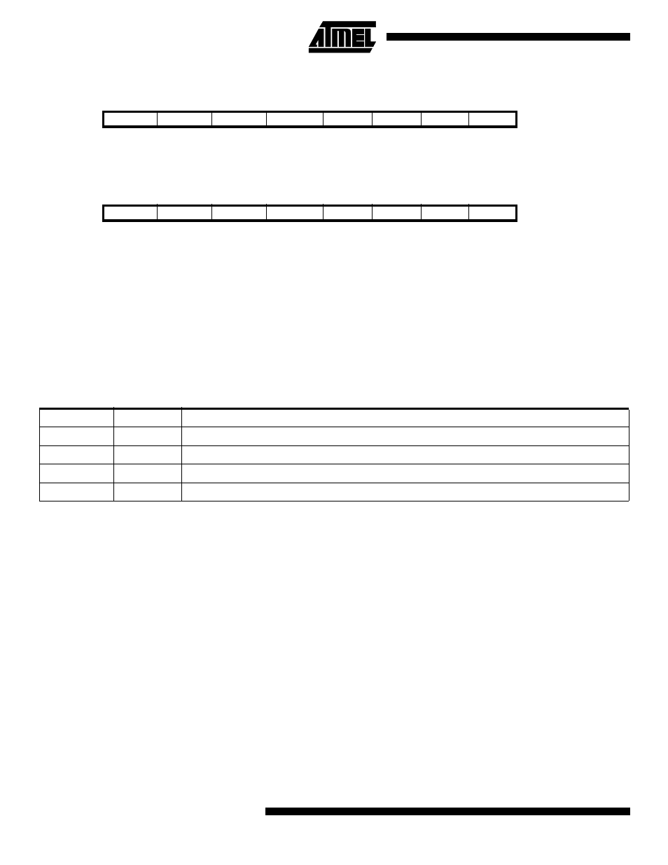
33 ($53)
-
PWM0
COM01
COM00
CTC0
CS02
CS01
CS00
TCCR0
Read/Write
R
R/W
R/W
R/W
R/W
R/W
R/W
R/W
Initial value
0
0
0
0
0
0
0
0
Bit
7
6
5
4
3
2
1
0
$25 ($45)
-
PWM2
COM21
COM20
CTC2
CS22
CS21
CS20
TCCR2
Read/Write
R
R/W
R/W
R/W
R/W
R/W
R/W
R/W
Initial value
0
0
0
0
0
0
0
0
Table 11. Compare Mode Select
COMn1
COMn0
Description
0
0
Timer/Counter disconnected from output pin OCn/PWMn
0
1
Toggle the OCn/PWMn output line.
1
0
Clear the OCn/PWMn output line (to zero).
1
1
Set the OCn/PWMn output line (to one).