Port c schematics, Port d, Port d data register - portd – Rainbow Electronics ATmega103L User Manual
Page 83
ATmega603/103
83
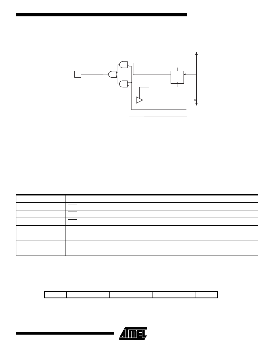
Port C Schematics
Figure 61. Port C Schematic Diagram (Pins PC0 - PC7)
Port D
Port D is an 8 bit bi-directional I/O port with internal pull-up resistors.
Three I/O memory address locations are allocated for the Port D, one each for the Data Register - PORTD, $12($32), Data
Direction Register - DDRD, $11($31) and the Port D Input Pins - PIND, $10($30). The Port D Input Pins address is read
only, while the Data Register and the Data Direction Register are read/write.
The Port D output buffers can sink 20 mA. As inputs, Port D pins that are externally pulled low will source current if the pull-
up resistors are activated.
Some Port D pins have alternate functions as shown in the following table:
When the pins are used for the alternate function the DDRD and PORTD register has to be set according to the alternate
function description.
Port D Data Register - PORTD
Table 32. Port D Pins Alternate Functions
Port Pin
Alternate Function
PD0
INT0 (External Interrupt0 Input)
PD1
INT1 (External Interrupt1 Input)
PD2
INT2 (External Interrupt2 Input)
PD3
INT3 (External Interrupt3 Input)
PD4
IC1 (Timer/Counter1 Input Capture Trigger)
PD6
T1 (Timer/Counter1 Clock Input)
PD7
T2 (Timer/Counter2 Clock Input)
Bit
7
6
5
4
3
2
1
0
$12
PORTD7
PORTD6
PORTD5
PORTD4
PORTD3
PORTD2
PORTD1
PORTD0
PORTD
Read/Write
R/W
R/W
R/W
R/W
R/W
R/W
R/W
R/W
Initial value
0
0
0
0
0
0
0
0
DA
T
A
B
US
D
Q
RESET
C
WP
PCn
R
WP:
RL:
A:
SRE:
n:
WRITE PORTC
READ PORTC LATCH
SRAM ADDRESS
EXTERNAL SRAM ENABLE
0-7
PORTCn
SRE
An
RL