Rainbow Electronics ATmega103L User Manual
Page 20
ATmega603/103
20
Note:
Reserved and unused locations are not shown in the table
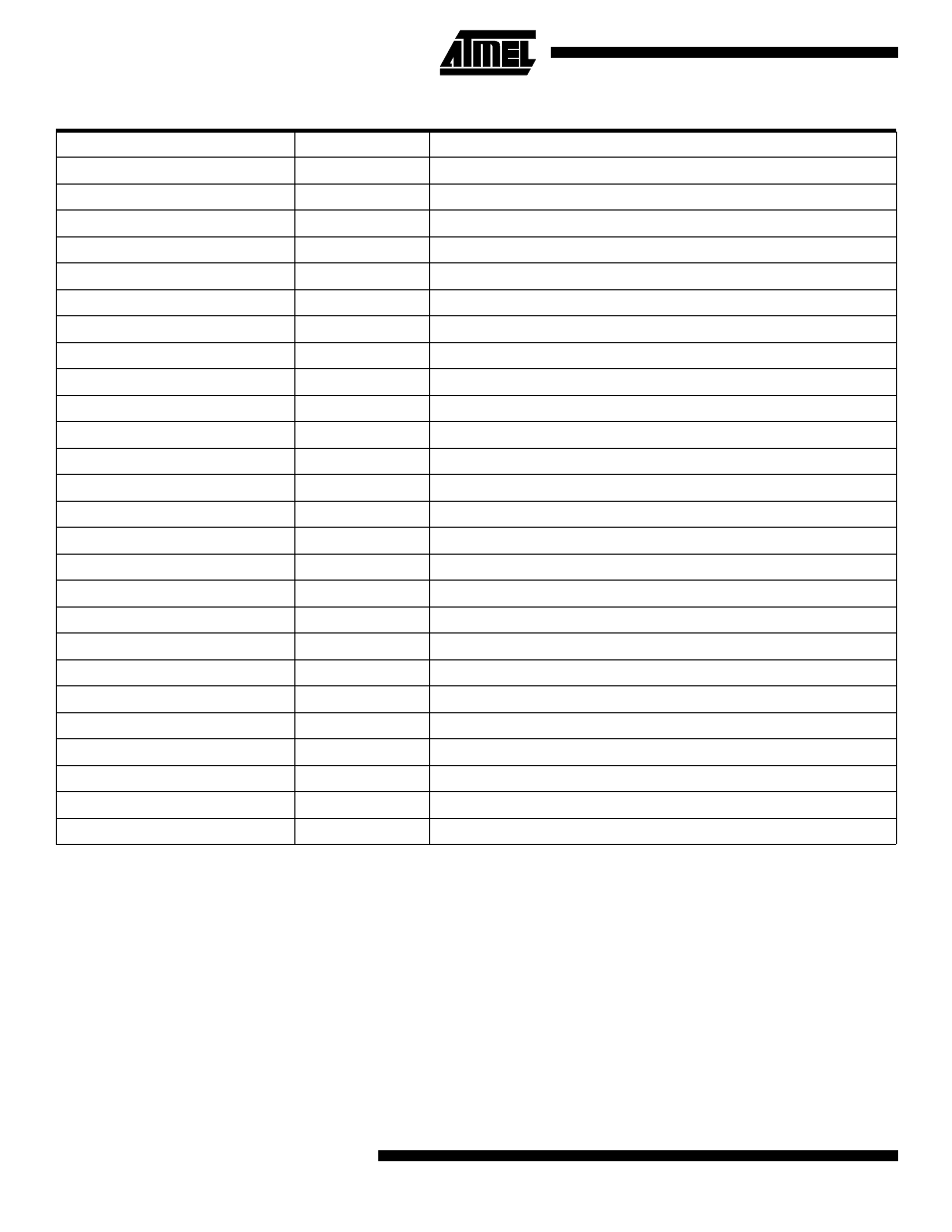
All the different ATmega603/103 I/Os and peripherals are placed in the I/O space. The different I/O locations are directly
accessed by the IN and OUT instructions transferring data between the 32 general purpose working registers and the I/O
space. I/O registers within the address range $00 - $1F are directly bit-accessible using the SBI and CBI instructions. In
these registers, the value of single bits can be checked by using the SBIS and SBIC instructions. Refer to the instruction
set chapter for more details. When using the I/O specific instructions IN, OUT, the I/O register address $00 - $3F are used.
When addressing I/O registers as SRAM, $20 must be added to this address. All I/O register addresses throughout this
document are shown with the SRAM address in parentheses.
For compatibility with future devices, reserved bits should be written to zero if accessed. Reserved I/O memory addresses
should never be written.
Some of the status flags are cleared by writing a logical one to them. Note that the CBI and SBI instructions will operate on
all bits in the I/O register, writing a one back into any flag read as set, thus clearing the flag. The CBI and SBI instructions
work with registers $00 to $1F only.
$1B ($3B)
PORTA
Data Register, Port A
$1A ($3A)
DDRA
Data Direction Register, Port A
$19 ($39)
PINA
Input Pins, Port A
$18 ($38)
PORTB
Data Register, Port B
$17 ($37)
DDRB
Data Direction Register, Port B
$16 ($36)
PINB
Input Pins, Port B
$15 ($35)
PORTC
Data Register, Port C
$12 ($32)
PORTD
Data Register, Port D
$11 ($31)
DDRD
Data Direction Register, Port D
$10 ($30)
PIND
Input Pins, Port D
$0F ($2F)
SPDR
SPI I/O Data Register
$0E ($2E)
SPSR
SPI Status Register
$0D ($2D)
SPCR
SPI Control Register
$0C ($2C)
UDR
UART I/O Data Register
$0B ($2B)
USR
UART Status Register
$0A ($2A)
UCR
UART Control Register
$09 ($29)
UBRR
UART Baud Rate Register
$08 ($28)
ACSR
Analog Comparator Control and Status Register
$07 ($27)
ADMUX
ADC Multiplexer Select Register
$06 ($26)
ADCSR
ADC Control and Status Register
$05 ($25)
ADCH
ADC Data Register High
$04 ($24)
ADCL
ADC Data Register Low
$03 ($23)
PORTE
Data Register, Port E
$02 ($22)
DDRE
Data Direction Register, Port E
$01 ($21)
PINE
Input Pins, Port E
$00 ($20)
PINF
Input Pins, Port F
Table 3. ATmega603/103 I/O Space (Continued)
I/O Address (SRAM Address)
Name
Function