Architectural overview – Rainbow Electronics ATmega103L User Manual
Page 7
ATmega603/103
7
Architectural Overview
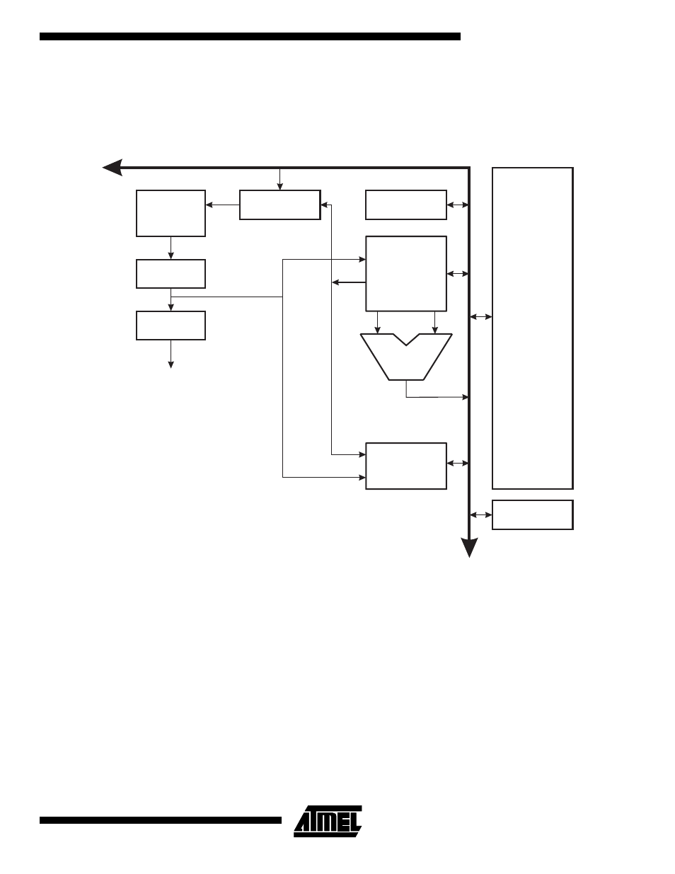
Figure 4. The ATmega603/103 AVR RISC Architecture
The AVR uses a Harvard architecture concept - with separate memories and buses for program and data. The program
memory is accesses with a single level pipeline. While one instruction is being executed, the next instruction is pre-fetched
from the program memory. This concept enables instructions to be executed in every clock cycle. The program memory is
in-system programmable Flash memory. With a few exceptions, AVR instructions have a single 16-bit word format,
meaning that every program memory address contains a single 16-bit instruction.
During interrupts and subroutine calls, the return address program counter (PC) is stored on the stack. The stack is
effectively allocated in the general data SRAM, and consequently the stack size is only limited by the total SRAM size and
the usage of the SRAM. All user programs must initialize the SP in the reset routine (before subroutines or interrupts are
executed). The 16-bit stack pointer SP is read/write accessible in the I/O space.
The 4000 bytes data SRAM can be easily accessed through the five different addressing modes supported in the AVR
architecture.
32K/64K x 16
Program
Memory
Instruction
Register
Instruction
Decoder
Program
Counter
Control Lines
32 x 8
General
Purpose
Registers
ALU
Status
and Test
2K/4K x 8
EEPROM
Peripherals
Data Bus 8-bit
AVR ATmega603/103 Architecture
4K x 8
Data
SRAM
DirectAddressing
IndirectAddressing