Adc dc characteristics, Interface to external sram – Rainbow Electronics ATmega103L User Manual
Page 72
ATmega603/103
72
ADC DC Characteristics
Notes:
1. Minimum for AV
CC
is 2.7V.
2. Maximum for AV
CC
is 6.0V.
Interface to external SRAM
The interface to the SRAM consists of:
• Port A: Multiplexed low-order address bus and data bus
• Port C: High-order address bus
• The ALE-pin: Address latch enable
• The RD and WR-pin: Read and write strobes.
The external data SRAM is enabled by setting the SRE - External SRAM enable bit of the MCUCR - MCU control register,
and will override the setting of the data direction register DDRA. When the SRE bit is cleared (zero), the external data
SRAM is disabled, and the normal pin and data direction settings are used. When SRE is cleared (zero), the address space
above the internal SRAM boundary is not mapped into the internal SRAM, as in AVR parts not having interface to the
external SRAM.
When ALE goes from high to low, there is a valid address on Port A. ALE is low during a data transfer. RD and WR are
active when accessing the external SRAM only.
When the external SRAM is enabled, the ALE signal may have short pulses when accessing the internal RAM, but the ALE
signal is stable when accessing the external SRAM.
Figure 50 sketches how to connect an external SRAM to the AVR using 8 latches which are transparent when G is high.
Default, the external SRAM access is a three-cycle scheme as depicted in Figure 51. When one extra wait state is needed
in the access cycle, set the SRW bit (one) in the MCUCR register. The resulting access scheme is shown in Figure 52. In
both cases, note that Port A is data bus in one cycle only. As soon as the data access finishes, Port A becomes a low order
address bus again.
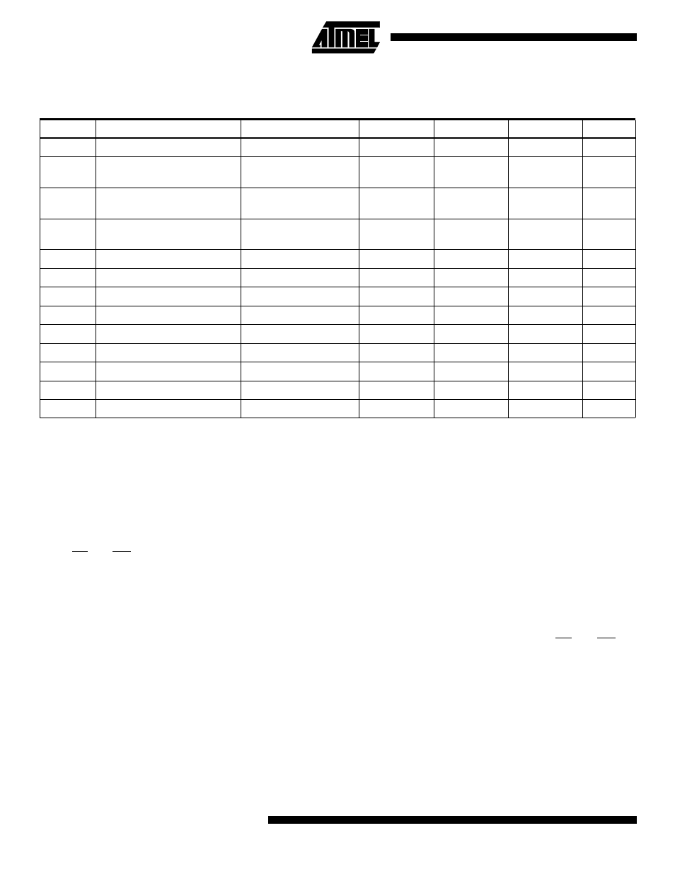
TA=-40°C to 85°C
Symbol
Parameter
Condition
Min
Typ
Max
Units
Resolution
10
Bits
Absolute accuracy
VREF = 4V, V
CC
= 4V
ADC clock = 200 kHz
1
2
LSB
Absolute accuracy
VREF = 4V, V
CC
= 4V
ADC clock = 1 MHz
4
LSB
Absolute accuracy
VREF = 4V, V
CC
= 4V
ADC clock = 2 MHz
16
LSB
Integral Non-Linearity
VREF > 2V
0.5
LSB
Differential Non-Linearity
VREF > 2V
0.5
LSB
Zero Error (Offset)
1
LSB
Conversion Time
70
280
µ
s
Clock Frequency
50
200
kHz
AV
CC
Analog Supply Voltage
V
CC
–0.3
V
CC
+0.3
V
V
REF
Reference Voltage
AGND
AV
CC
V
R
REF
Reference Input Resistance
6
10
13
k
Ω
R
AIN
Analog Input Resistance
100
M
Ω