External clock drive waveforms, Figure 78 – Rainbow Electronics ATmega103L User Manual
Page 109
ATmega603/103
109
Figure 78. External RAM Timing
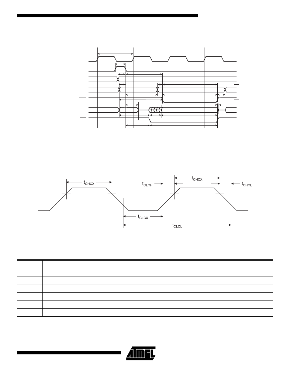
External Clock Drive Waveforms
Figure 79. External Clock Drive Waveforms
Table 50. External Clock Drive
Note:
See “External Data Memory Timing” on page 107 for a description of how the duty cycle influences the timing for the External
Data Memory
Symbol
Parameter
V
CC
= 2.7V to 3.6V
V
CC
= 4.0V to 5.5V
Units
1/t
CLCL
Oscillator Frequency
0
4
0
6
MHz
t
CLCL
Clock Period
250
167
ns
t
CHCX
High Time
100
67
ns
t
CLCX
Low Time
100
67
ns
t
CLCH
Rise Time
1.6
0.5
µ
s
t
CHCL
Fall Time
1.6
0.5
µ
s
System Clock O
ALE
WR
RD
Data / Address [7..0]
Data / Address [7..0]
Address [15..8]
Address
Address
Address
T1
T2
T3
T4
Prev. Address
Prev. Address
Prev. Address
1
0
4
2
13
3a
5
Note: Clock cycle T3 is only present when external SRAM waitstate is enabled
10
12
14
15
11
8
9
16
7
6
3b
Data
Data
Wr
ite
Read
Addr.
Addr.
VIL1
VIH1
- MAX5151 (16 pages)
- MAXQ3108 (64 pages)
- MAX5661 (39 pages)
- MAX6691 (7 pages)
- MAX5362 (12 pages)
- ADC10158 (26 pages)
- MAX8922L (14 pages)
- MAX8596Z (8 pages)
- MAX7491 (18 pages)
- MAX15040 (15 pages)
- MAX5177 (16 pages)
- ADC08138 (22 pages)
- MAX5961 (42 pages)
- T89C51RD2 (86 pages)
- MAX16055 (9 pages)
- MAX6659 (17 pages)
- ADC0820 (20 pages)
- MAX6678 (19 pages)
- MAX8884Z (15 pages)
- MAX16915 (9 pages)
- MAX8620 (18 pages)
- MAX5144 (12 pages)
- MAX6670 (8 pages)
- MAX8760 (39 pages)
- W78C32C (14 pages)
- MX7533 (8 pages)
- MAX8727 (13 pages)
- MAX9053 (15 pages)
- W78C54 (16 pages)
- MAX8614B (15 pages)
- W90N740 (219 pages)
- MAX6626 (13 pages)
- ADC10738 (30 pages)
- MAX17000 (31 pages)
- MAX5051 (21 pages)
- MAXQ1004 (18 pages)
- MAX6871 (51 pages)
- MX7847 (12 pages)
- MAX6608 (6 pages)
- MAX17083 (15 pages)
- MAX6641 (17 pages)
- MAX5251 (16 pages)
- MAX6338 (8 pages)
- MAX6690 (16 pages)
- MAX8668 (18 pages)