I/o-ports, Port a, Figure 52 – Rainbow Electronics ATmega103L User Manual
Page 74
ATmega603/103
74
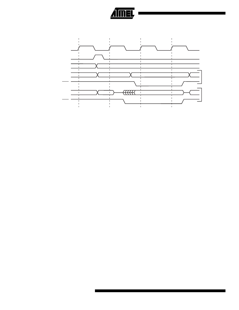
Figure 52. External SRAM Access Cycle with wait state
I/O-Ports
All AVR ports have true Read-Modify-Write functionality when used as general digital I/O ports. This means that the direc-
tion of one port pin can be changed without unintentionally changing the direction of any other pin with the SBI and CBI
instructions. The same applies for changing drive value (if configured as output) or enabling/disabling of pull-up resistors (if
configured as input).
Port A
Port A is an 8-bit bi-directional I/O port with internal pull-ups.
Three I/O memory address locations are allocated for Port A, one each for the Data Register - PORTA, $1B($3B), Data
Direction Register - DDRA, $1A($3A) and the Port A Input Pins - PINA, $19($39). The Port A Input Pins address is read
only, while the Data Register and the Data Direction Register are read/write.
All port pins have individually selectable pull-up resistors. The Port A output buffers can sink 20mA and thus drive LED
displays directly. When pins PA0 to PA7 are used as inputs and are externally pulled low, they will source current if the
internal pull-up resistors are activated.
The Port A pins have alternate functions related to the optional external data SRAM. Port A can be configured to be the
multiplexed low-order address/data bus during accesses to the byte.
When Port A is set to the alternate function by the SRE - External SRAM Enable - bit in the MCUCR - MCU Control Regis-
ter, the alternate settings override the data direction register.
System Clock Ø
ALE
WR
RD
Data / Address [7..0]
Data / Address [7..0]
Address [15..8]
Address
Address
Address
T1
T2
T3
T4
Prev. Address
Prev. Address
Prev. Address
Data
Data
Wr
ite
Read
Addr.
Addr.