Common control and status registers – Rainbow Electronics DS21458 User Manual
Page 71
DS21455/DS21458 Quad T1/E1/J1 Transceivers
71 of 270
12. COMMON CONTROL AND STATUS REGISTERS
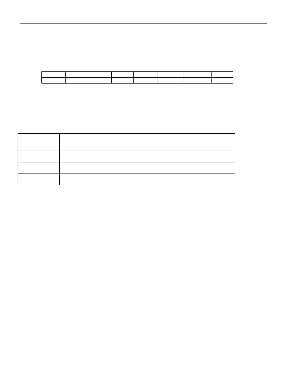
Register Name:
CCR1
Register Description:
Common Control Register 1
Register Address:
70h
Bit #
7
6
5
4
3
2
1
0
Name —
CRC4R
SIE
ODM
—
TCSS1
TCSS0
RLOSF
Default 0 0 0 0 0 0
0 0
Bit 0/Function of the RLOS/LOTC Output (RLOSF).
0 = Receive Loss of Sync (RLOS)
1 = Loss of Transmit Clock (LOTC)
Bit 1/Transmit Clock Source Select Bit 0 (TCSS0).
Bit 2/Transmit Clock Source Select Bit 1 (TCSS1).
TCSS1 TCSS0
TRANSMIT CLOCK SOURCE
0
0
The TCLK pin is always the source of transmit clock.
0 1
Switch to the clock present at RCLK when the signal at the TCLK pin fails to transition
after one channel time.
1
0
Use the scaled signal present at MCLK as the transmit clock. The TCLK pin is ignored.
1
1
Use the signal present at RCLK as the transmit clock. The TCLK pin is ignored.
Bit 3/Unused, must be set to zero for proper operation.
Bit 4/Output Data Mode (ODM).
0 = pulses at TPOSO and TNEGO are one full TCLKO period wide
1 = pulses at TPOSO and TNEGO are 1/2 TCLKO period wide
Bit 5/Signaling Integration Enable (SIE).
0 = signaling changes of state reported on any change in selected channels
1 = signaling must be stable for three multiframes for a change of state to be reported
Bit 6/CRC-4 Recalculate (CRC4R) (E1 Only).
0 = transmit CRC-4 generation and insertion operates in normal mode
1 = transmit CRC-4 generation operates according to G.706 Intermediate Path Recalculation method
Bit 7/ Unused, must be set to zero for proper operation.