Rainbow Electronics DS21458 User Manual
Page 114
DS21455/DS21458 Quad T1/E1/J1 Transceivers
114 of 270
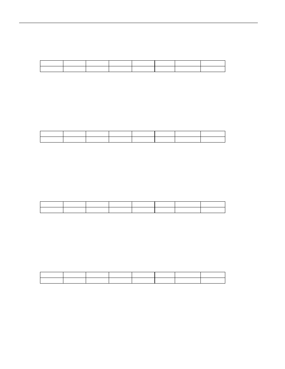
Register Name:
RCBR3
Register Description:
Receive Channel Blocking Register 3
Register Address:
8Ah
Bit
# 7 6 5 4 3 2 1 0
Name CH24 CH23 CH22 CH21 CH20 CH19 CH18 CH17
Default
0 0 0 0 0 0 0 0
Bits 0 to 7/Receive Channels 17 to 24 Channel Blocking Control Bits (CH17 to CH24).
0 = force the RCHBLK pin to remain low during this channel time
1 = force the RCHBLK pin high during this channel time
Register Name:
RCBR4
Register Description:
Receive Channel Blocking Register 4
Register Address:
8Bh
Bit
# 7 6 5 4 3 2 1 0
Name CH32 CH31 CH30 CH29 CH28 CH27 CH26 CH25
Default
0 0 0 0 0 0 0 0
Bits 0 to 7/Receive Channels 25 to 32 Channel Blocking Control Bits (CH25 to CH32).
0 = force the RCHBLK pin to remain low during this channel time
1 = force the RCHBLK pin high during this channel time
Register Name:
TCBR1
Register Description:
Transmit Channel Blocking Register 1
Register Address:
8Ch
Bit
# 7 6 5 4 3 2 1 0
Name CH8 CH7 CH6 CH5 CH4 CH3 CH2 CH1
Default
0 0 0 0 0 0 0 0
Bits 0 to 7/Transmit Channels 1 to 8 Channel Blocking Control Bits (CH1 to CH8).
0 = force the TCHBLK pin to remain low during this channel time
1 = force the TCHBLK pin high during this channel time
Register Name:
TCBR2
Register Description:
Transmit Channel Blocking Register 2
Register Address:
8Dh
Bit
# 7 6 5 4 3 2 1 0
Name CH16 CH15 CH14 CH13 CH12 CH11 CH10 CH9
Default
0 0 0 0 0 0 0 0
Bits 0 to 7/Transmit Channels 9 to 16 Channel Blocking Control Bits (CH9 to CH16).
0 = force the TCHBLK pin to remain low during this channel time
1 = force the TCHBLK pin high during this channel time