Receive level indicator, Receive g.703 section 10 synchronization signal, Monitor mode – Rainbow Electronics DS21458 User Manual
Page 160: Figure 25-3. typical monitor application
DS21455/DS21458 Quad T1/E1/J1 Transceivers
160 of 270
There are two ranges of receive sensitivity for both T1 and E1, which is selectable by the user. The EGL
bit of LIC1 (LIC1.4) selects the full or limited sensitivity.
The resultant E1 or T1 clock derived from MCLK is multiplied by 16 via an internal PLL and fed to the
clock recovery system. The clock recovery system uses the clock from the PLL circuit to form a 16 times
over-sampler, which is used to recover the clock and data. This oversampling technique offers
outstanding performance to meet jitter tolerance specifications shown in
Normally, the clock that is output at the RCLK pin is the recovered clock from the E1 AMI/HDB3 or T1
AMI/B8ZS waveform presented at the RTIP and RRING inputs. If the jitter attenuator is placed in the
receive path (as is the case in most applications), the jitter attenuator restores the RCLK to an
approximate 50% duty cycle. If the jitter attenuator is either placed in the transmit path or is disabled, the
RCLK output can exhibit slightly shorter high cycles of the clock. This is due to the highly over-sampled
digital clock recovery circuitry. See the Receive AC Timing Characteristics section for more details.
When no signal is present at RTIP and RRING, a receive carrier loss (RCL) condition will occur and the
RCLK will be derived from the JACLK source.
25.2.1 Receive Level Indicator
The DS21455/DS21458 will report the signal strength at RTIP and RRING in 2.5dB increments via RL3-
RL0 located in the Information Register 2 (INFO2). This feature is helpful when trouble shooting line
performance problems.
25.2.2 Receive G.703 Section 10 Synchronization Signal
The DS21455/DS21458 can receive a 2.048MHz square-wave synchronization clock as specified in
Section 10 of ITU G.703. To use this mode, set the receive synchronization clock enable (LIC3.2) = 1.
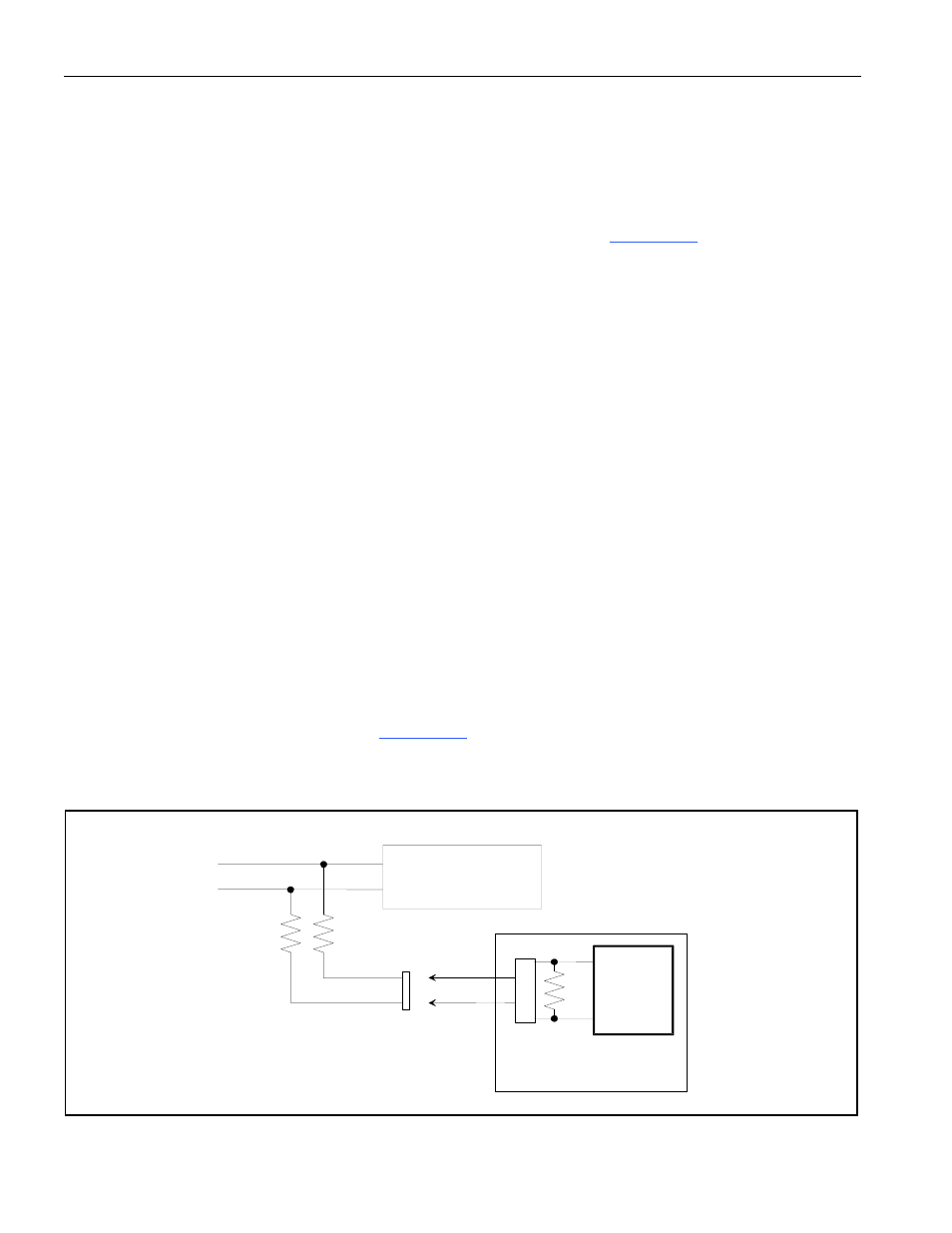
25.2.3 Monitor Mode
Monitor applications in both E1 and T1 require various flat gain settings for the receive-side circuitry.
The DS21455/DS21458 can be programmed to support these applications via the monitor mode control
bits MM1 and MM0 in the LIC3 register.
depicts a typical monitor-mode application.
Figure 25-3. Typical Monitor Application
MONITOR
PORT JACK
T1/E1 LINE
X
F
M
R
DS21455/
DS21458
Rt
Rm
Rm
SECONDARY T1/E1
TERMINATING DEVICE
PRIMARY T1/E1
TERMINATING
DEVICE