A/d converter – Panasonic MN103001G/F01K User Manual
Page 365
A/D Converter
14-11
S/H
bp9 bp8
bp7
bp6 bp5 bp4
bp3 bp2 bp1
bp0
S/H
bp9 bp8
bp7
bp6 bp5 bp4
bp3 bp2 bp1
bp0
S/H
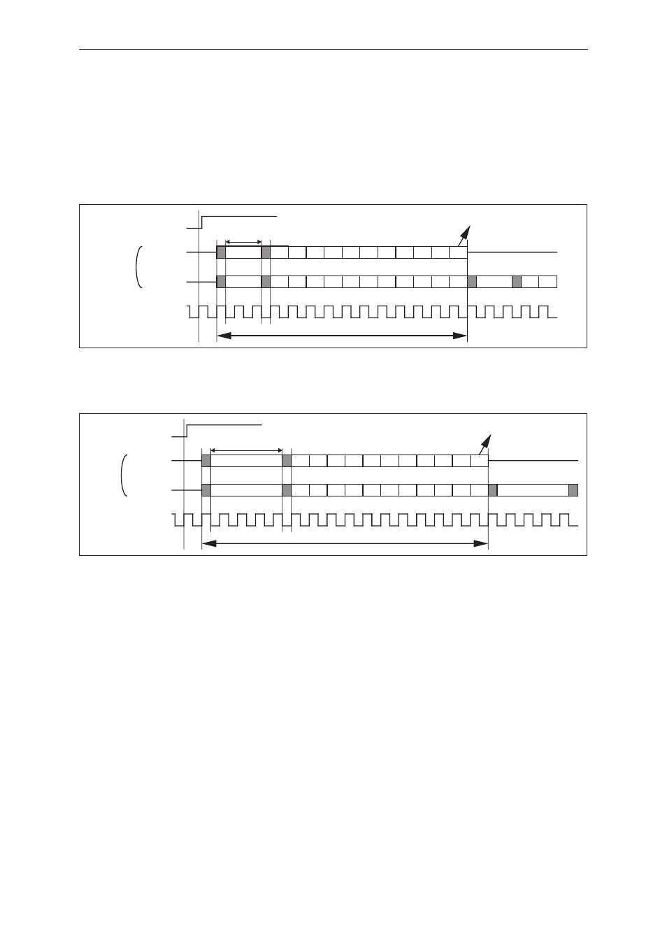
16 (= 12 +4) cycles
ADEN flag
Conversion
reference clock
Status
One-time
conversion
Continuous
conversion
Sampling cycle
• Interrupt request
• Write to data buffer
Transfer
Transfer
■
Conversion reference clock selection, sampling cycle number selection
The A/D conversion time is [(12 + number of sampling cycles) x IOCLK/clock selection]/channel.
For example, if the conversion reference clock is set as 1/8 of IOCLK and the number of sampling cycles is set as
two cycles, the A/D conversion time is IOCLK x 112 cycles/channel.
Fig. 14-5-5 Conversion Timing When Using Two Sampling Cycles
Fig. 14-5-6 Conversion Timing When Using Four Sampling Cycles
Set the conversion reference clock so that one cycle is at least 200 ns.
Set the number of sampling cycles so that one sampling cycle is at least 400 ns (when the output impedance
of the external device that drives the AN pin is 1 k
Ω
or less).
If the output impedance of the external device that drives the AN pin is greater than 1 k
Ω
, it is necessary to
lengthen the sampling cycle.
When A/D conversion (ADEN = "1") is started up from the stopped state (ADEN = "0"), a wait state of a
maximum of one conversion reference clock cycle is inserted between the point when ADEN goes to "1" and the
actual start of conversion.
S/H
bp9
bp8 bp7
bp6 bp5 bp4
bp3 bp2 bp1
bp0
S/H
bp9
bp8 bp7
bp6 bp5 bp4
bp3 bp2 bp1
bp0
S/H
bp9
bp8
14 (= 12 +2) cycles
ADEN flag
Conversion
reference clock
Status
One-time
conversion
Continuous
conversion
Sampling cycle
• Interrupt request
• Write to data buffer
Transfer
Transfer