Panasonic MN103001G/F01K User Manual
Page 181
Bus Controller (BC)
8-67
MCLK
Row
CAO+1
An
CAS
RE
Dn
ASR
RASn
Column
CAS
ASC
Column
CAS
Column
CAS
ASC
ASC
MCLK
Row
CAO+1
An
CAS
WEn
Dn
ASR
RASn
Column
Column
CAS
ASC
ASC
CAS
ASC
CAS
Column
(a)
Read Timing
(b)
Write Timing
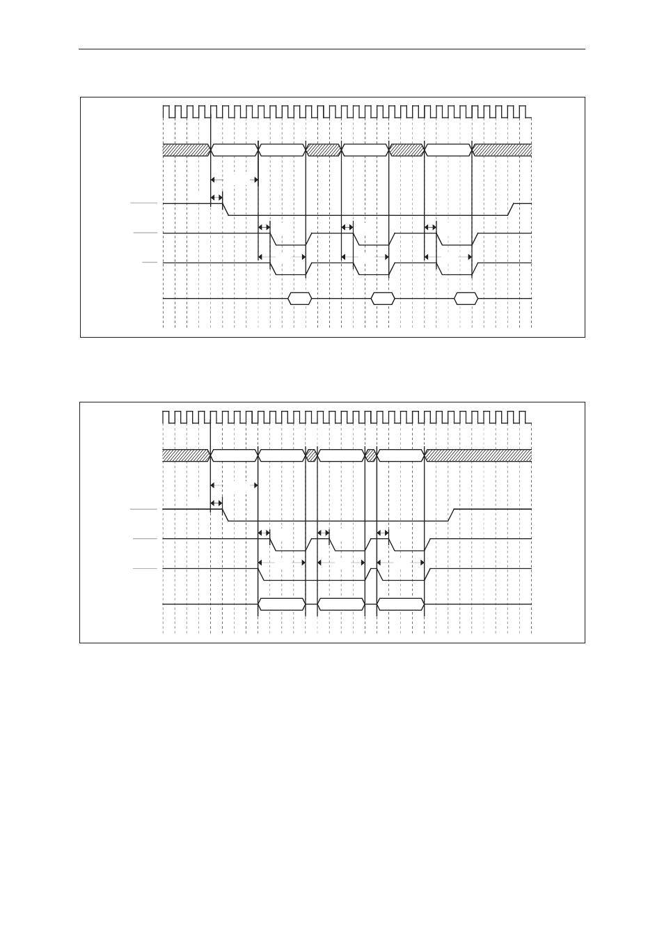
Fig. 8-14-6
Software Page Mode Read/Write Timing
For details on the various timing settings, refer to the description of the memory control register in section 8.6,
“Description of Registers.”