10 bus cycle – Panasonic MN103001G/F01K User Manual
Page 143
Bus Controller (BC)
8-29
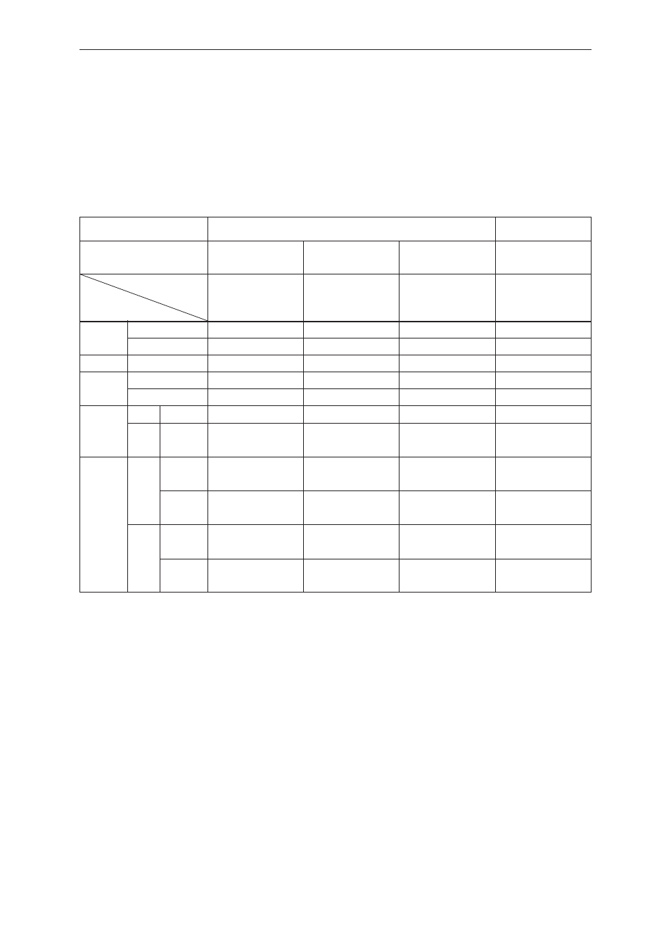
8.10 Bus Cycle
Depending on the value of the external input pin CKSEL and the internal registers, the MCLK frequency can be
either 1/2, 1, 2, or 4 times the input frequency, and the IOCLK frequency can be either 1/8, 1/4, 1/2, or 1 times the
input frequency. Note that SYSCLK is output with either 1/2 or 1 times the input frequency.
Table 8-10-1
Relationship between the Clock Frequency and
the Number of Cycles (CPU Cycles) Required for Access
CKSEL
H
L
MCK [1:0] =10
MCK [1:0] = 01
MCK [1:0] = 00
(Not using)
4
2
1
1/2
Instruction read
2
2
2
2
Data read
3
3
3
3
Read/write
1
1
1
1
Read
3
3
3
3
Write
2
2
2
2
Internal
Read
Synchronous
7 to 10
7 to 10
7 to 10
7
(*3)
I/O
(*1)
(*3)
Write
Synchronous
6 to 9
6 to 9
6 to 9
6
External
(*2)
Number of EX bus
Number of EX bus
Number of EX bus
Number of EX bus
memory
Read
Synchronous
cycles + 3 to 6
cycles + 3 to 4
cycles + 3
cycles + 3
Asyn-
Number of EX bus
Number of EX bus
Number of EX bus
Number of EX b
us
chronous
cycles + 3
cycles + 3
cycles + 3
cycles + 3
(*1)
(*2)
Number of EX bus
Number of EX bus
Number of EX bus
Number of EX bus
Write
Synchronous
cycles + 2 to 5
cycles + 2 to 3
cycles + 2
cycles + 2
Asyn-
Number of EX bus
Number of EX bus
Number of EX bus
Number of EX bus
chronous
cycles +2
cycles + 2
cycles + 2
cycles +2
(*1)
If the store buffer is operational, the writing to internal I/O and external memory is entirely performed with
0 wait states.
(*2)
In the synchronous mode, a synchronization wait of a maximum of 3 cycles or of 1 cycle is generated when
the MCLK frequency is four times or two times the SYSCLK frequency, respectively.
(*3)
Because the ratio of IOCLK to MCLK is always 1/4, a wait for synchronization is inserted.
Clock control register
MCK [1:0] = 11 is prohibited.
Control
register in
BC
Internal
instruction
ROM/Internal
flash memory
Internal data
RAM
Destination
of access
MCLK/Input
frequency