8 clock control register – Panasonic MN103001G/F01K User Manual
Page 138
Bus Controller (BC)
8-24
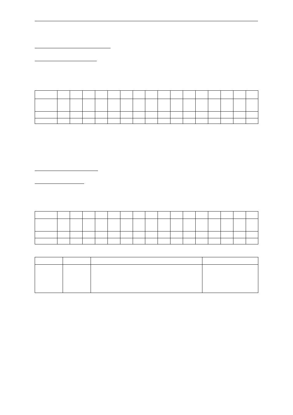
8.6.7 Page Row Address Register
Page Row Address Register
Register symbol: PRAR
Address:
x'32000044
Purpose:
Sets the row address for DRAM software page mode.
Bit No.
15
14
13
12
11
10
9
8
7
6
5
4
3
2
1
0
Bit
PRAR PRAR PRAR PRAR PRAR PRAR PRAR PRAR PRAR PRAR PRAR PRAR PRAR PRAR PRAR PRAR
name
15
14
13
12
11
10
9
8
7
6
5
4
3
2
1
0
Reset
X
X
X
X
X
X
X
X
X
X
X
X
X
X
X
X
Access
R/W
R/W
R/W
R/W
R/W
R/W
R/W
R/W
R/W
R/W
R/W R/W
R/W
R/W
R/W
R/W
When DRAM software page mode is initiated (i.e., when the PE bit in memory control register 1B/2B is set to “1”),
the contents of the page row address register are output as the row address.
Set the row address in the page row address register before initiating DRAM software page mode. The row address
that is set at this point should have already been subjected to the shift operation in accordance with the DRAM size.
8.6.8 Clock Control Register
Clock Control Register
Register symbol: CKCTR
Address:
x'32004000
Purpose:
Sets the internal clock multiplier, etc.
Bit No.
15
14
13
12
11
10
9
8
7
6
5
4
3
2
1
0
Bit name
–
–
–
–
–
–
–
–
–
–
–
–
–
–
MCK MCK
name
1
0
Reset
0
0
0
0
0
0
0
0
0
0
0
0
0
0
0
0
Access
R
R
R
R
R
R
R
R
R
R
R
R
R
R
R/W
R/W
Bit No.
Bit name
Description
Setting conditions
1 to 0
MCK1 to 0
MCLK frequency setting for the input frequency
00:
1x
01:
2x
10:
4x
11:
prohibited
For details, refer to Chapter 6, “Clock Generator.”