Honeywell DCP552 Mark II User Manual
Page 132
7-33
●
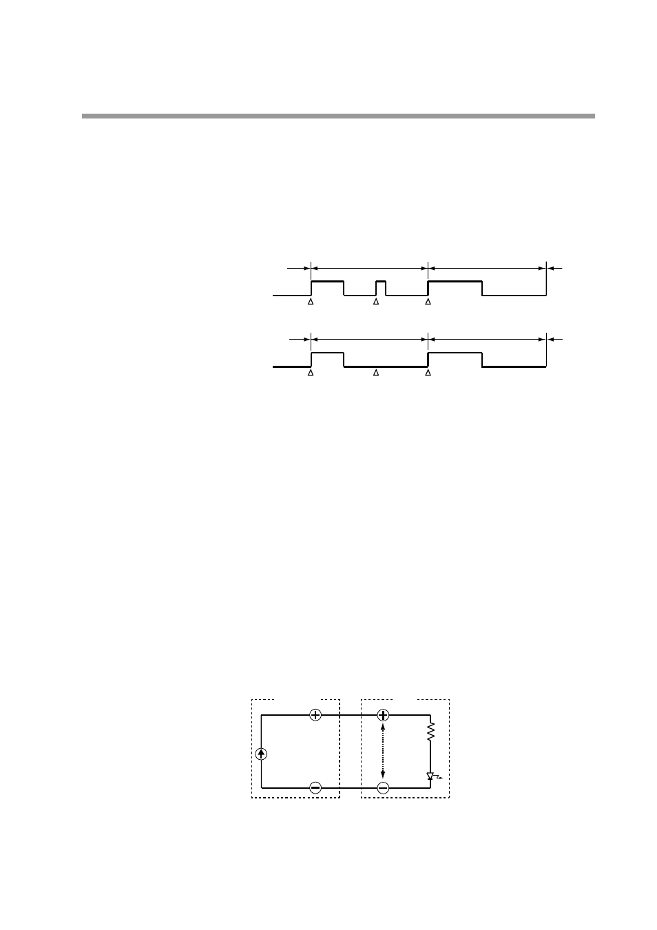
C93 (time proportional output system)
●
C94 (time proportional output system)
0: Goes on again within time proportional cycle
1: Does not go on again within time proportional cycle
• This setting determines whether the output is to go on again after the result of a
PID computation has changed in a time proportional cycle (cycle time) and the
output has been turned off.
• The difference between the two settings is illustrated below.
●
C95 (voltage output control)
●
C96 (voltage output control)
In a voltage time proportional output driven by SSR, the
DCP552
must enter the
SSR rated input voltage (optimum striking voltage of arc).
The
DCP552
employs a newly developed variable output system that can output
optimum striking voltage of arc to accommodate multiple SSR drives. A suitable
current value is set on the
DCP552
to obtain optimum striking voltage of arc for
the internal impedance of the SSR. An equivalent circuit with related equations is
shown below.
• Description of symbols
(1) Settings
I
0
: set
DCP552
output current (range: 2 to 22mA)
V
0
: end-to-end load voltage (13.2V)
V
SSR'
: actual voltage input to SSR
V
SSR
: rated input voltage range for SSR (V
SSR/MIN
to V
SSR/MAX
)
V
SSR/MIN
: minimum SSR rated input voltage
V
SSR/MAX
: maximum SSR rated input voltage
Z
: internal SSR impedance
V
D
: internal SSR voltage drop (normally about 1 to 2V)
(2) Equivalent circuit showing connection of one SSR
Equations (1) and (2) below must be satisfied.
V
SSR/MIN
≤ I
0
× Z + V
D
≤V
0
Equation (1)
V
SSR'
≤ V
SSR/MAX
Equation (2)
(V
SSR'
= I
0
× Z + V
D
)
I
(V )
0
0
DCP552
SSR
V
SSR'
Z
V
D
When set to 0
20%
→
50%
→
40%
OFF
ON
PID computation
result
Cycle time
Cycle time
20%
→
50%
→
40%
OFF
ON
PID computation
result
When set to 1
Cycle time
Cycle time
Chapter 7. PARAMETER SETUP