Port 1, General i/o mode – Zilog Z86193 User Manual
Page 55
Z8
®
CPU
User Manual
UM001604-0108
Input/Output Ports
48
DAV0 (P32) and RDY0 (P35) when Port 0 is an input port, or RDY0 (P32) and DAV0
(P35) when Port 0 is an output port (see
Handshake direction is determined by the configuration (input or output) assigned to the
Port 0 upper nibble:P04–P07. The lower nibble must have the same I/O configuration as
the upper nibble to be under handshake control.
on page 46 displays the Port 0
upper and lower nibbles and the associated handshake lines of Port 3.
Port 1
This section describes only the I/O operation. The port's external memory interface opera-
tion is discussed later in this manual.
on page 45 displays a block diagram of
Port 1.
General I/O Mode
Port 1 can be an 8-bit, bidirectional, CMOS or TTL compatible port with multiplexed
address (A7–A0) and data (D7–D0) ports. These eight I/O lines can be byte programmed
as inputs or outputs or can be configured under software control as an Address/Data port
for interfacing to external memory. The input buffers can be Schmitt-Triggered, level-
shifted, or a single-point buffer. In some cases, the output buffers can be globally pro-
grammed as either push–pull or open-drain. Low-EMI output buffers can be globally pro-
grammed by software, as an OTP program option, or as a ROM Mask Option. In some
cases, the Z8
®
MCU can have autolatches hardwired to the inputs. Refer to specific prod-
uct specifications for exact input/output buffer-type features available (see
and
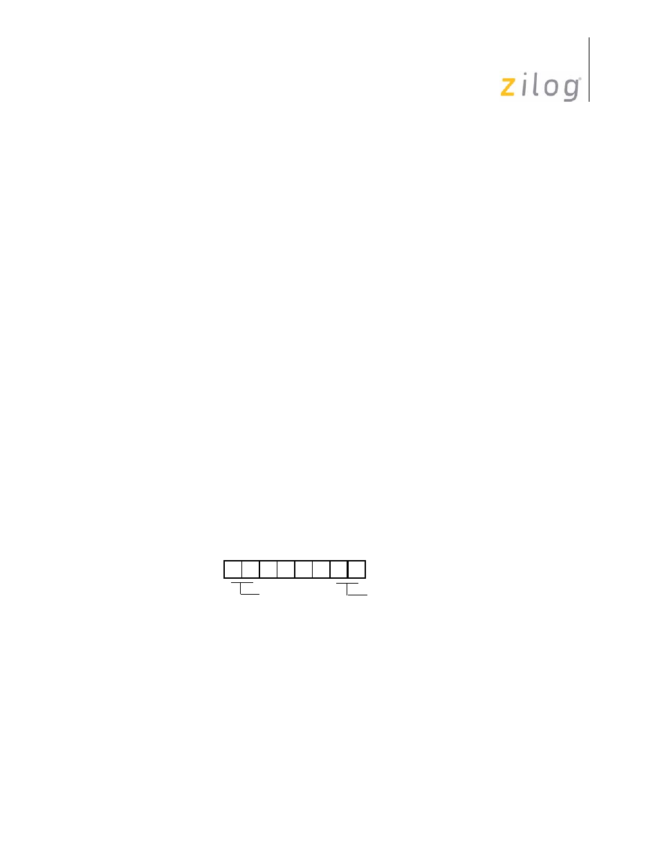
Figure 32. Port 0 I/O Operation
D7 D6 D1 D0
(Write-Only)
01 = Input
1X = A8–A11
P00–P03 Mode
00 = Output
Port 0–1 Mode Register (P01M)
Register F8h (P01M)
P04–P07 Mode
00 = Output
01 = Input
1X = A12–A15
- Z86233 Z86243 Z86733 Z86743 Z86C02 Z86C04 Z86C08 Z86C15 Z86C21 Z86C30 Z86C31 Z86C33 Z86C36 Z86C40 Z86C43 Z86C61 Z86C62 Z86C63 Z86C65 Z86C83 Z86C90 Z86C91 Z86C93 Z86C96 Z86E02 Z86E03 Z86E04 Z86E06 Z86E07 Z86E08 Z86E15 Z86E21 Z86E30 Z86E31 Z86E33 Z86E34 Z86E40 Z86E43 Z86E44 Z86E61 Z86E63 Z86E83 Z86K15 Z86L02 Z86L04 Z86L08 Z86L16 Z8E000 Z8E001 Z8PE003