Address strobe, Data strobe, Address strobe data strobe – Zilog Z86193 User Manual
Page 143: Figure 127
Z8
®
CPU
User Manual
UM001604-0108
External Interface
136
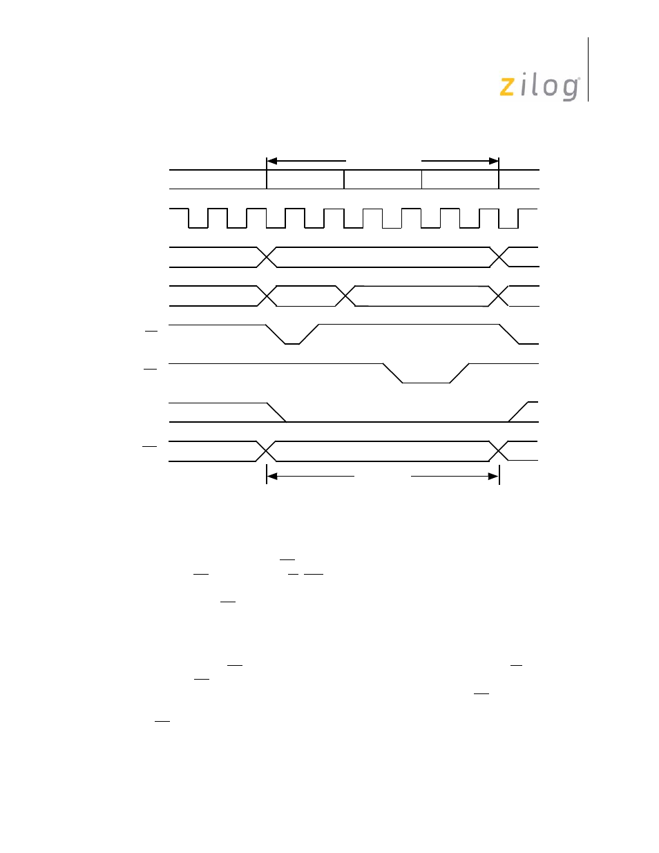
Address Strobe
All transactions start with AS driven Low and then raised High by Z8
®
CPU. The rising
edge of AS indicates that R/W, DM (if used), and the address outputs are valid. The
address outputs (AD7–AD0), remain valid only during MnT1 and typically must be
latched using AS. Address outputs (A15–A8) remain stable throughout the machine cycle,
regardless of the addressing mode.
Data Strobe
Z8
®
CPU uses DS to time the actual data transfer. For Write operations (R/W = Low), a
Low on DS indicates that valid data is on the AD7–AD0 lines. For Read operations (R/W
= High), the bus is placed in a high-impedance state before driving DS Low, so the
addressed device can put its data on the bus. The Z8 CPU samples this data prior to raising
DS High.
Figure 127. External Memory Write Cycle
Machine Cycle
T1
T2
T3
Clock
A15-A8
AD7–AD0
AS
DS
R/W
DM
Write Cycle
A8-A15
A7–A0
D7–D0 OUT
- Z86233 Z86243 Z86733 Z86743 Z86C02 Z86C04 Z86C08 Z86C15 Z86C21 Z86C30 Z86C31 Z86C33 Z86C36 Z86C40 Z86C43 Z86C61 Z86C62 Z86C63 Z86C65 Z86C83 Z86C90 Z86C91 Z86C93 Z86C96 Z86E02 Z86E03 Z86E04 Z86E06 Z86E07 Z86E08 Z86E15 Z86E21 Z86E30 Z86E31 Z86E33 Z86E34 Z86E40 Z86E43 Z86E44 Z86E61 Z86E63 Z86E83 Z86K15 Z86L02 Z86L04 Z86L08 Z86L16 Z8E000 Z8E001 Z8PE003